LED package for backlight unit

a backlight unit and led technology, applied in the field of backlight units, can solve the problems of poor power consumption efficiency, excessive power consumption, and the majority of power consumed by the backlight unit, and achieve the effect of preventing the deformation of the led packag

Active Publication Date: 2007-01-02
SAMSUNG ELECTRONICS CO LTD
View PDF6 Cites 69 Cited by
  • Summary
  • Abstract
  • Description
  • Claims
  • Application Information

AI Technical Summary

Benefits of technology

[0017]Accordingly, the present invention has been made keeping in mind the above problems occurring in the prior art, and an object of the present invention is to provide an LED package for a backlight unit, which is capable of maintaining high image quality as well as increasing luminous efficiency using LEDs in a display device, such as an LCD.
[0018]Another object of the present invention is to provide an LED package for a backlight unit, which has an optimal arrangement structure so as to allow the LED package not only to use many LEDs but also to have a thin and long shape.
[0019]Another object of the present invention is to provide an LED package for a backlight unit, which is capable of preventing physical deformation or breakage due to an external impact or the like in the case where the casing of the LED package is formed of a thin and long injection-molded body.
[0025]Preferably, the LED package for a backlight unit may further include at least one support that is formed to traverse the length of the LED package and prevents the deformation of the LED package.

Problems solved by technology

Meanwhile, in the case where such a backlight unit is applied to portable products, such as a mobile communication terminal, most of the power is consumed by the backlight unit.
The CCFL and the EEFL are disadvantageous in that they have poor power consumption efficiencies and, therefore, consume excessive power.
As a result, the case where the conventional LED packages 10 are used as a backlight is disadvantageous in that light is nonuniformly incident on the LCD 20, so that a stain phenomenon occurs on the LCD 20, thus degrading image quality.

Method used


Image

  • LED package for backlight unit
  • LED package for backlight unit
  • LED package for backlight unit

Examples


Embodiment Construction

[0035]Reference now should be made to the drawings, in which the same reference numerals are used throughout the different drawings to designate the same or similar components.

[0036]FIG. 3 is a perspective view of an LED package for a backlight unit in accordance with an embodiment of the present invention.

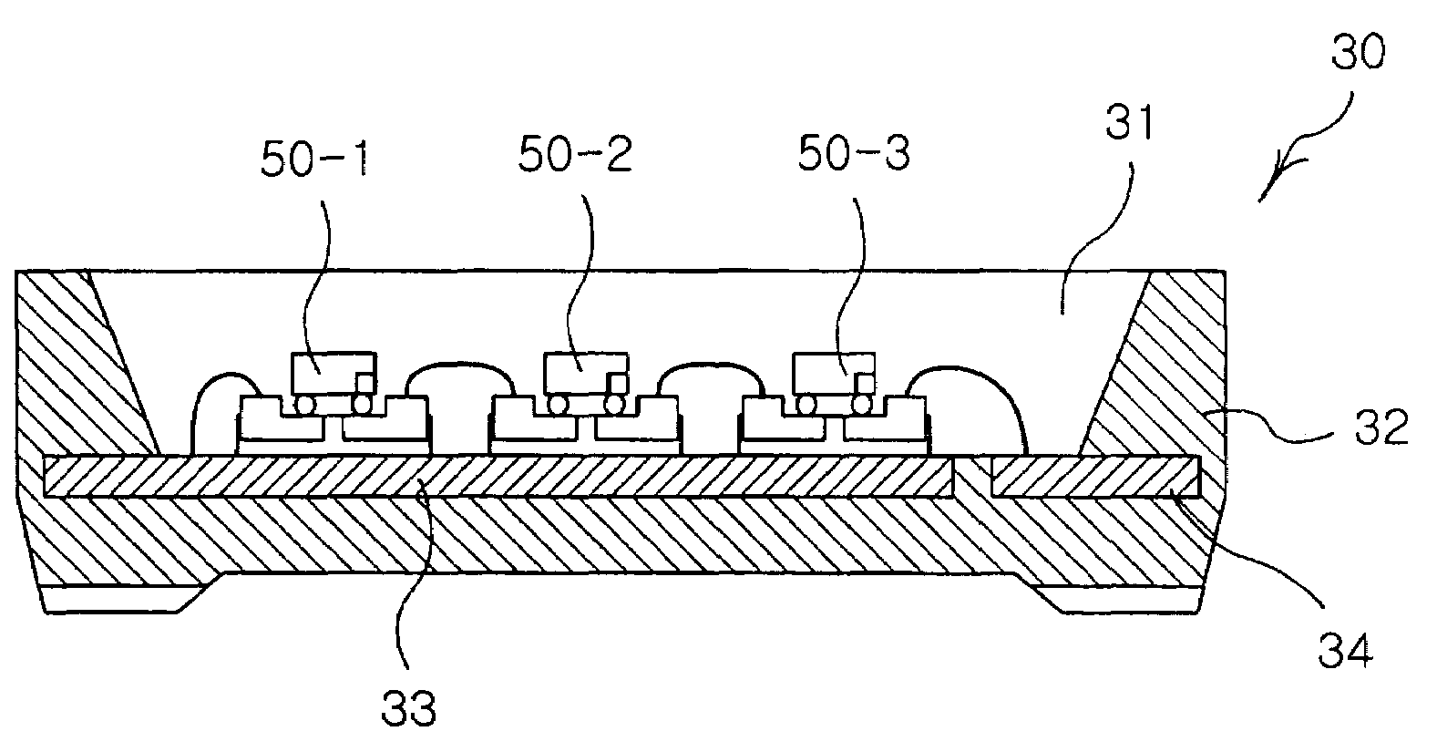
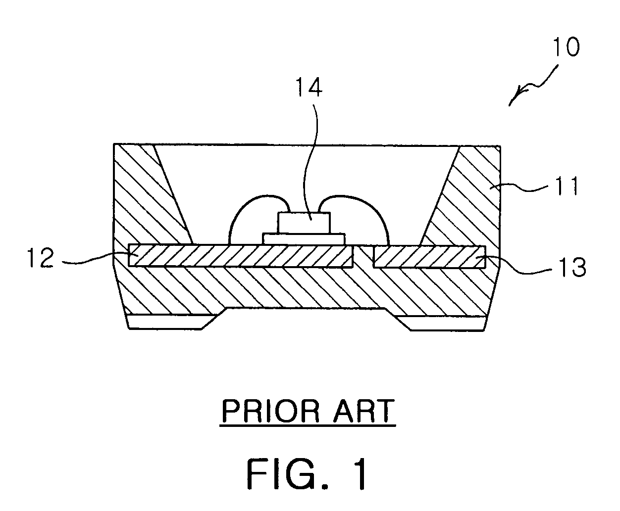
[0037]Referring to FIG. 3, the LED package 10 for a backlight unit according to an embodiment of the present invention includes a body 32 provided with a cavity 31, two electrode plates 33 and 34 formed in the cavity 31, and a plurality of LED chips 35. In this case, the two electrode plates 33 and 34 may be classified into a die bonding part 33 and a wire bonding part 34.

[0038]The LED package 30 may be used on, for example, one side of an LCD mounted in a portable terminal. Accordingly, the LED package 10 is thin in thickness t, and is considerably long in length l, compared to the thickness t, to correspond to the length of the LCD of the portable table.

[0039]The plurality of LE...


PUM

PropertyMeasurementUnit
operating voltageaaaaaaaaaa
wavelength bandaaaaaaaaaa
transparentaaaaaaaaaa

Abstract

Disclosed herein is an LED package for a backlight unit. The LED package includes a plurality of LEDs, a die bonding part, a wire bonding part and a body. The die bonding part, on which the plurality of LEDs is arranged, allows the first electrodes of the LEDs to be electrically connected to an external circuit. The wire bonding part is spaced apart from the die bonding part by a predetermined distance to be insulated from the die bonding part and allows the second electrodes of the LEDs to be electrically connected to the external circuit so that the LEDs are operated. The body has a molding cup which is used to fill a space above the LEDs with transparent resin and a base on which the die bonding part and the wire bonding part are arranged.

Description

RELATED APPLICATION[0001]The present application is based on, and claims priority from, Korean Application Number 2004-0059324, filed Jul. 28, 2004, the disclosure of which is hereby incorporated by reference herein in its entirety.BACKGROUND OF THE INVENTION[0002]1. Field of the Invention[0003]The present invention relates generally to a backlight unit that is used as the light emitting source of a display device, such as a liquid crystal display, and, more particularly, to a backlight unit that uses light emitting diodes as a light emitting source.[0004]2. Description of the Related Art[0005]With the development of the electronic device industry, not only a variety of small-sized and low-energy-consumption display devices but also imaging apparatuses, computers and mobile communication terminals using the display devices are being developed. Liquid Crystal Displays (LCDs), which were developed to meet such a trend, are being popularized as display devices for monitors and mobile c...

Claims


Application Information

Patent Timeline
Patent Type & Authority Patents(United States)
IPC IPC(8): F21V21/00H01L33/48
CPCH01L25/0753H01L33/486H01L2224/48091H01L2224/48137H01L2224/48247H01L2924/00014
Inventor HAN, KYUNG TAEGPARK, CHAN WANGLEE, SEON GOO
Owner SAMSUNG ELECTRONICS CO LTD
Why Eureka
Try Eureka