Multi-layer wiring structure with dummy patterns for improving surface flatness

a multi-layer wiring and dummy pattern technology, applied in the direction of electrical equipment, semiconductor devices, semiconductor/solid-state device details, etc., can solve the problems of affecting the inability to dispose of dummy pattern dummy patterns just under the inductor, and the likely formation of erosion in this area, so as to eliminate the influence of dummy pattern on the functional element and improve the flatness of the surface after cmp

Active Publication Date: 2007-01-09
FUJITSU SEMICON LTD
View PDF4 Cites 33 Cited by
  • Summary
  • Abstract
  • Description
  • Claims
  • Application Information

AI Technical Summary

Benefits of technology

[0011]An object of this invention is to provide a multi-layer wiring structure capable of improving the flatness of a surface after CMP even if there is an area not allowed to form conductive patterns.
[0014]Since conductive patterns are not formed in the first area where a functional element is disposed, the influence of the conductive patterns upon the functional element can be eliminated. By disposing dummy patterns in the second or fourth areas, the flatness of a surface after CMP can be improved.

Problems solved by technology

If the pattern density of a wiring layer is not uniform, the surface flatness after CMP is likely to be degraded.
Further, it is not appropriate to dispose conductive dummy patterns just under an inductor.
The pattern density of an area of a wiring layer under the inductor becomes therefore low so that erosion is likely to be formed in this area.
These problems occur not only when a functional element formed on an upper layer is an inductor but also when a functional element is formed which does not allow a conductive pattern to be formed just under the functional element.

Method used


Image

  • Multi-layer wiring structure with dummy patterns for improving surface flatness
  • Multi-layer wiring structure with dummy patterns for improving surface flatness
  • Multi-layer wiring structure with dummy patterns for improving surface flatness

Examples


Embodiment Construction

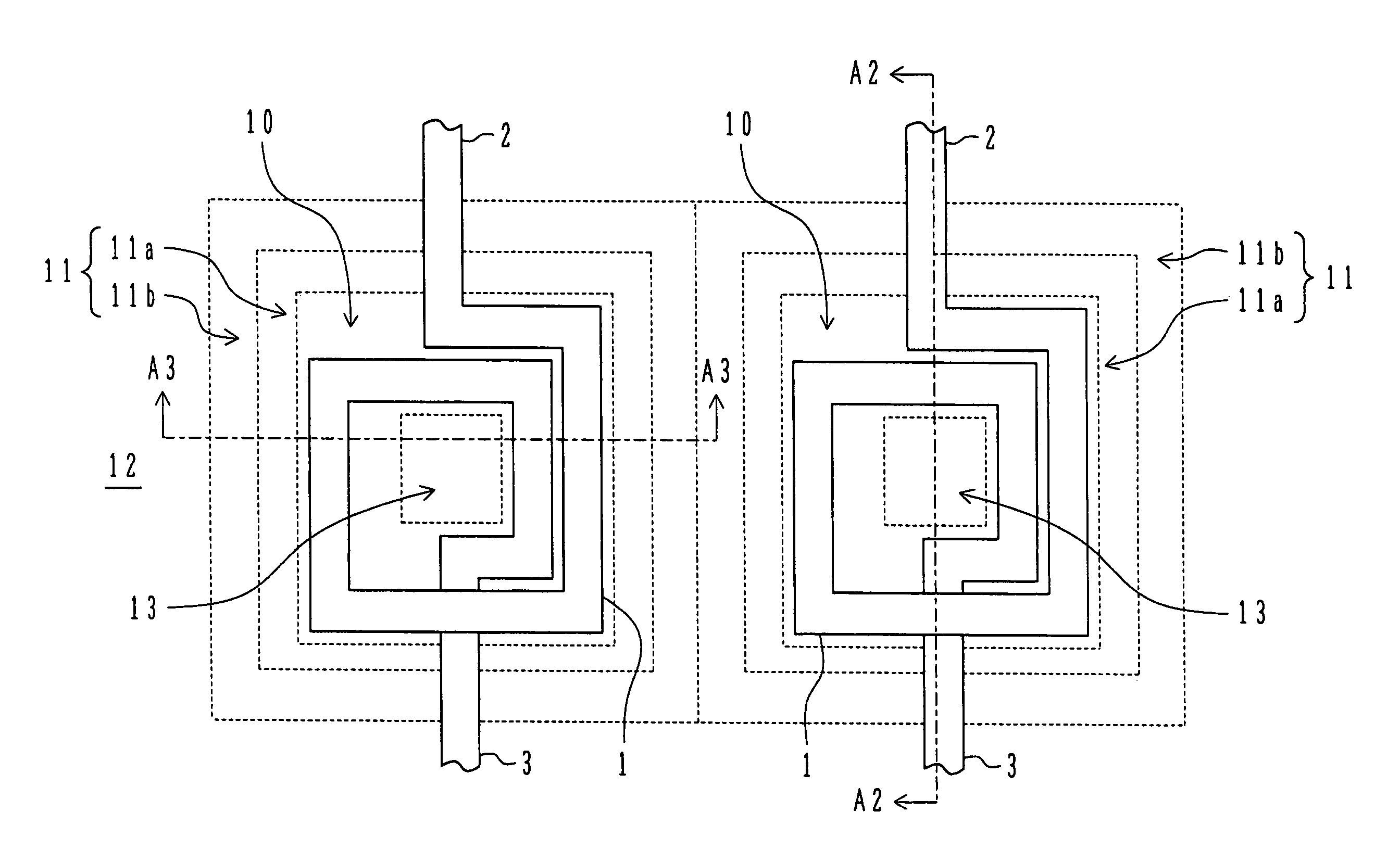
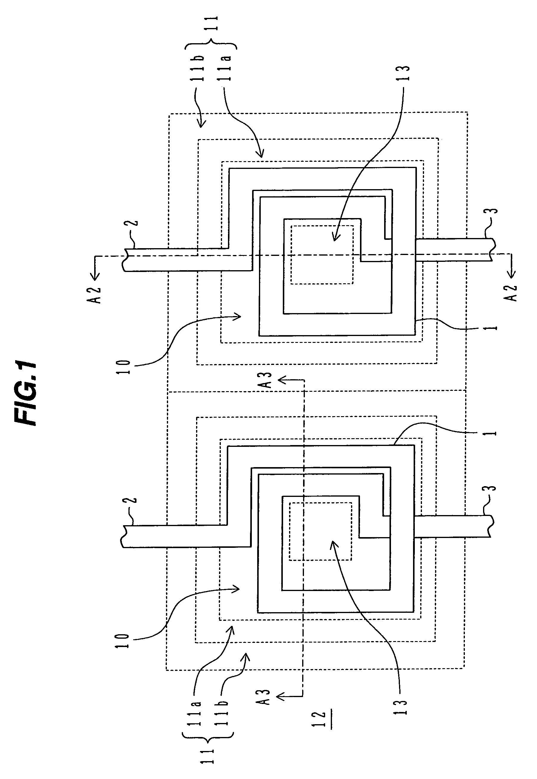
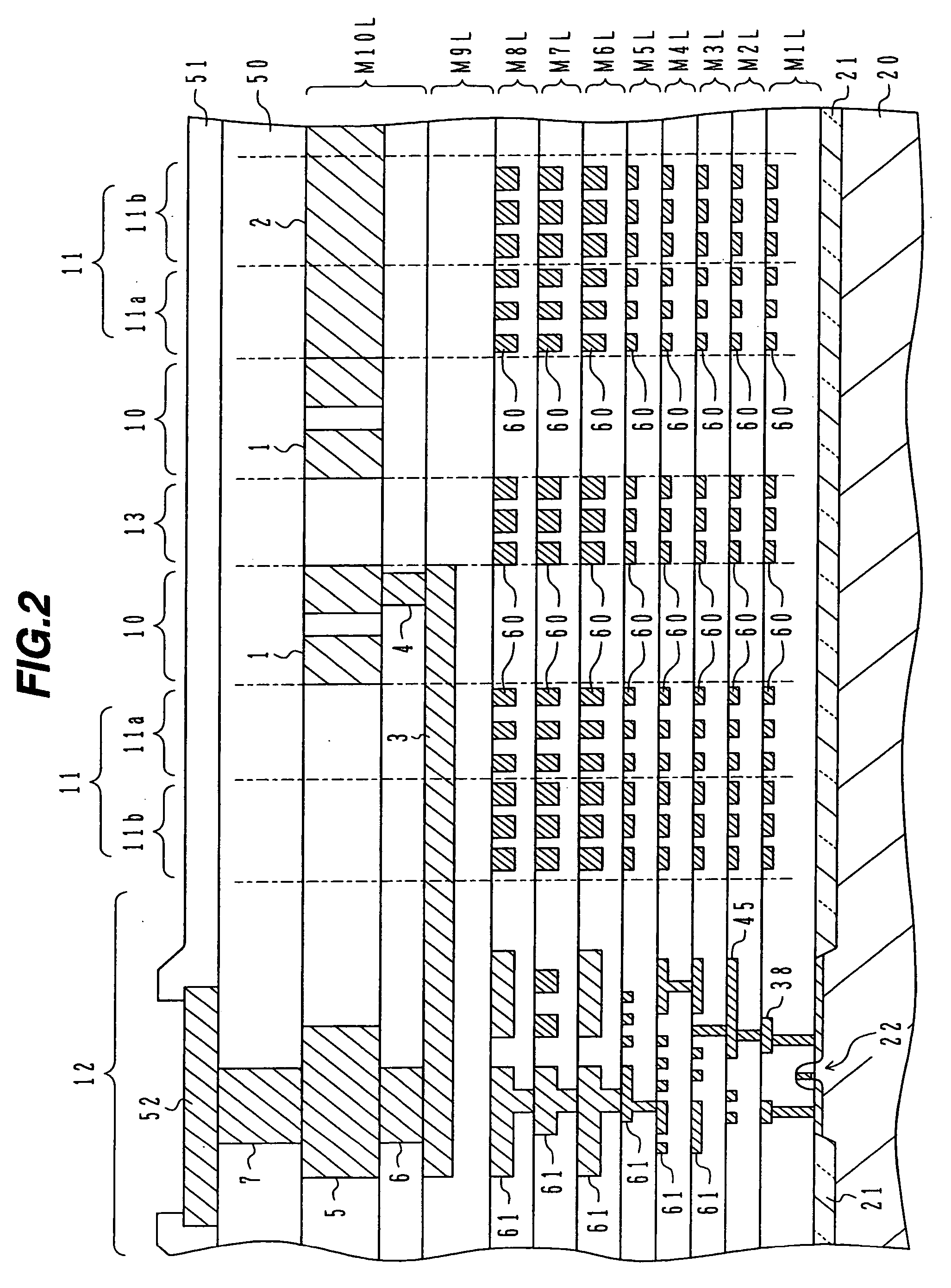
[0024]FIG. 1 is a partial plan view of a semiconductor device having a multi-layer wiring structure according to an embodiment. A loop-shape first area 10 where an inductor is disposed is defined on a substrate surface. In the outer area of the first area 10, a second area 11 is defined surrounding the first area 10. The second area 11 has a first sub area 11a (an inner peripheral side thereof) of the first area 10 and a second sub area 11b outside of the first sub area 11a (an outer peripheral side thereof).

[0025]An inner periphery of the first area 10, a border between the first area 10 and the second area 11, a border between the first sub area 11a and the second sub area 11b, and an outer periphery of the second area 11 have, for example, a square shape or a rectangle shape. If a plurality of inductors are disposed, a plurality of second areas 11 are defined. Two second areas 11 are disposed in contact with each other by sharing a portion of the outer peripheries thereof.

[0026]A...


PUM


Abstract

A first area, a ring shape second area surrounding the first area, and a third area surrounding the second area are defined on the surface of a support substrate. A first wiring layer is disposed above the support substrate. A wiring is formed in the third area, dummy patterns being formed in the second area, and conductive patterns are not formed in the first area. A functional element is disposed above the first wiring layer and in the first area.

Description

CROSS REFERENCE TO RELATED APPLICATION[0001]This application is based on and claims priority of Japanese Patent Application No. 2004-095535 filed on Mar. 29, 2004, the entire contents of which are incorporated herein by reference.BACKGROUND OF THE INVENTION[0002]A) Field of the Invention[0003]The present invention relates to a multi-layer wiring structure, and more particularly to a multi-layer wiring structure having dummy patterns for improving flatness of the surface of a wiring layer.[0004]B) Description of the Related Art[0005]Brief description will be made on a damascene method of forming multi-layer wiring of a semiconductor integrated circuit device. After an interlayer insulating film is formed, wiring trenches and via holes are formed in the interlayer insulating film. A conductive film of copper or the like is formed to fill the via holes and wiring trenches with the conductive film. If necessary, a barrier metal layer is formed to prevent diffusion of copper. The conduct...

Claims


Application Information

Patent Timeline
Patent Type & Authority Patents(United States)
IPC IPC(8): H01L23/48H01L21/3205H01L21/027H01L21/768H01L21/822H01L23/52H01L23/522H01L27/04H01L29/00
CPCH01L21/7684H01L23/5227H01L2924/0002H01L2924/00
Inventor KARASAWA, TOSHIYUKIOTSUKA, SATOSHI
Owner FUJITSU SEMICON LTD
Why Eureka
Try Eureka