Flexible ZnO based thin film transistor and preparation method thereof

A technology of thin film transistors and flexible substrates, applied in the direction of transistors, semiconductor/solid-state device manufacturing, semiconductor devices, etc., can solve the problems of not using photolithographic patterns, poor surface flatness, not using panels, etc., to enhance operability and use Reliability, enhanced water and oxygen barrier properties, improved operability and stability

Inactive Publication Date: 2013-11-27
FUDAN UNIV
View PDF5 Cites 19 Cited by
  • Summary
  • Abstract
  • Description
  • Claims
  • Application Information

AI Technical Summary

Problems solved by technology

However, the current plastic substrate has poor surface flatness, and micron-scale protrusions on the surface will cause damage to the device and poor reliability; and the water and oxygen transmission rates are high, and the device is prone to aging
At the same time, due to the different thermal expansion coefficients of different film layers in the process of transistor preparation, the growth of the film, heat treatment, etc. will cause bending shrinkage and other effects on it.

Method used


Image

  • Flexible ZnO based thin film transistor and preparation method thereof
  • Flexible ZnO based thin film transistor and preparation method thereof

Examples


Embodiment 1

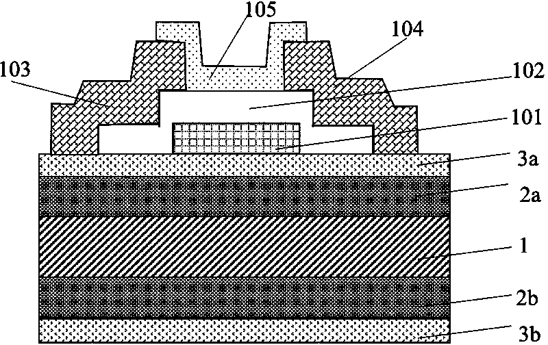
[0046] Such as figure 1 As shown, the manufacturing process of the bottom gate of the present invention, the bottom contact zinc oxide thin film transistor comprises the following steps:

[0047] a) Pretreatment of flexible substrates;

[0048] b) Depositing a gate electrode film (101) by a Lift-off process;

[0049] c) depositing gate insulating material (102);

[0050] d) forming a gate insulating layer pattern by photolithography;

[0051] e) Depositing source and drain electrodes (103, 104) by Lift-off process;

[0052] f) spin-coating an inorganic solution to obtain a ZnO semiconductor layer (105);

[0053] g) Obtain the channel region pattern by photolithographic wet etching.

[0054] In step a), the pretreatment of the flexible substrate is the same as above.

[0055] The lift-off process in the step b) is specifically, using Ruihong positive resist, spin-coating at 5000rpm for 30s, pre-baking at 95°C for 10min, exposing for 40s, developing for 20-40s, and post-ba...

Embodiment 2

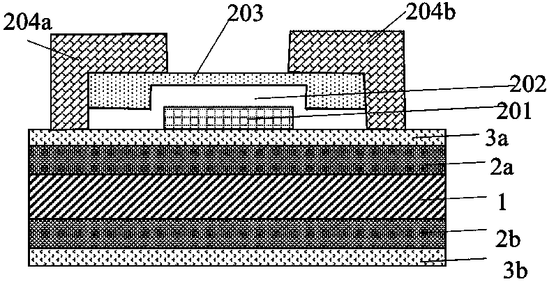
[0076] Preparation method of bottom gate and top contact TFT: 1, substrate pretreatment; 2, depositing gate electrode 201; 3, depositing gate insulating layer 202; 4, depositing ZnO semiconductor channel layer 203; 5, depositing Product source and drain (204a, 204b). In this method, the gate insulating layer and the channel layer can be etched simultaneously with a set of photolithography plates to form patterns, and the gate electrode, source and drain electrodes are made by Lift-off process, and this structure can avoid the influence of the annealing process on the source and drain electrodes.


PUM


Abstract

The invention belongs to the technical field of microelectronic and flat panel display, and particularly relates to a flexible ZnO based thin film transistor and a preparation method thereof. The flexible thin film transistor comprises a flexible substrate, a flat layer, an isolation buffer layer, a gate, a gate insulating layer, a source electrode, a drain electrode and semiconductor channel layers. N type and P type zinc oxide semiconductor channel layers are prepared by using a simple inorganic solution method, and the temperature of the whole process is controlled within 200 DEG C. When in manufacturing, the flat layer and the isolation buffer layer with the same thickness are grown at two sides of the substrate, the flexible substrate bending in the process is alleviated through a thermal annealing mode, and the subsequent lithography alignment accuracy is improved. According to the transistor and the preparation method, the maneuverability and stability of the flexible TFT and subsequent devices can be improved, the preparation process is simple, and the production cost is low.

Description

technical field [0001] The invention belongs to the technical field of microelectronics and flat panel display, and in particular relates to a structure of a flexible ZnO-based thin film transistor (Thin Film Transistor, TFT) and a preparation method thereof. Background technique [0002] The development of contemporary display technology requires higher-performance thin-film transistors (TFTs) to drive LCD pixels and AMOLED pixels. At present, the channel materials widely used in thin-film transistors are amorphous silicon (a-Si: H) and polysilicon. Amorphous silicon TFT has the advantages of simple preparation process and good uniformity, but its mobility is low (< 1cm 2 / V s), which cannot meet the driving requirements of current AMOLED displays; although low-temperature polysilicon TFTs have high mobility (> 10cm 2 / V·s), but it requires laser-assisted annealing and the manufacturing cost is high, and the mass production uniformity of polycrystalline materials is ...

Claims


Application Information

Patent Timeline
Patent Type & Authority Applications(China)
IPC IPC(8): H01L29/786H01L29/06H01L21/34
Inventor 繁萌李辉瞿敏妮仇志军刘冉
Owner FUDAN UNIV
Why Eureka
Try Eureka