Structure and method for fabricating a magnetic thin film memory having a high field anisotropy

a magnetic thin film and high field anisotropy technology, applied in the direction of nanomagnetism, coating, electrical apparatus, etc., can solve the problems of weak uniaxial anisotropy, weak hk magnetic material, and limited range over which the magnitude of hsub>k-shape /sub>can be varied, etc., to achieve high hk magnetic material, low critical current, and high energy barrier to thermal reversal

Inactive Publication Date: 2012-01-19
EVERSPIN TECHNOLOGIES
View PDF2 Cites 54 Cited by
  • Summary
  • Abstract
  • Description
  • Claims
  • Application Information

AI Technical Summary

Benefits of technology

[0011]A thin-film magnetic device having a high HK magnetic material, a high energy barrier to thermal reversal, a low critical current in

Problems solved by technology

However, there are several drawbacks to relying on HK-shape to provide Hsw.
Variations in Hsw translate into a smaller operating window for programming of the bits using a magnetic field and are therefore undesirable.
Third, the range over which the magnitude of HK-shape can be varied is limited.
Only certain bit shapes produce reliable switching and although varying the thickness of the film will vary HK-shape, there is a maximum bit thickness above which the bit switching quality degrades due to domain formation.
Such an oblique deposition can, under the right conditions, produce an asymmetry in the microstructure of the film that results in a strong uniaxial anisotropy.
However, the oblique deposition also results in a large nonuniformity of the film thicknes

Method used


Image

  • Structure and method for fabricating a magnetic thin film memory having a high field anisotropy
  • Structure and method for fabricating a magnetic thin film memory having a high field anisotropy
  • Structure and method for fabricating a magnetic thin film memory having a high field anisotropy

Examples


Embodiment Construction

[0027]The following detailed description is merely illustrative in nature and is not intended to limit the embodiments of the subject matter or the application and uses of such embodiments. Any implementation described herein as exemplary is not necessarily to be construed as preferred or advantageous over other implementations. Furthermore, there is no intention to be bound by any expressed or implied theory presented in the preceding technical field, background, brief summary, or the following detailed description.

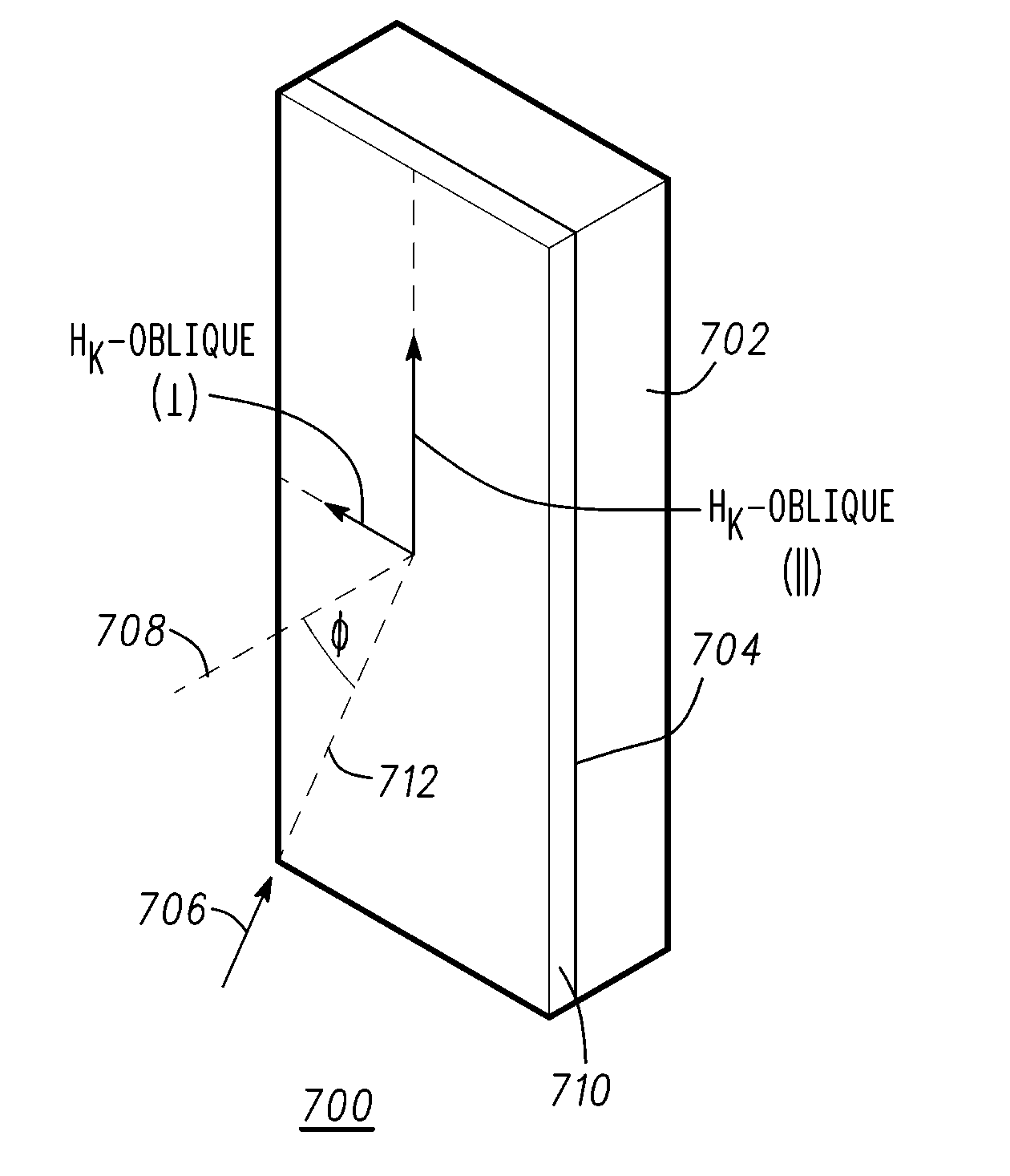
[0028]The embodiments described herein include a new MRAM structure, and method of manufacture of the structure, having a magnetic free layer deposited in two or more static oblique deposition steps from opposed directions. For example, a first oblique deposition may be performed, the structure rotated 180 degrees, and a second oblique deposition is performed. Various exemplary embodiments include optional smooth magnetic and / or non-magnetic layers that prevent diffusion...


PUM


Abstract

A method for depositing uniform and smooth ferromagnetic thin films with high deposition-induced microstructural anisotropy includes a magnetic material deposited in two or more static oblique deposition steps from opposed directions to form a free layer having a high kink Hk, a high energy barrier to thermal reversal, a low critical current in spin-torque switching embodiments, and improved resistance to diffusion of material from adjacent layers in the device. Nonmagnetic layers deposited by the static oblique deposition technique may be used as seed layers for a ferromagnetic free layer or to generate other types of anisotropy determined by the deposition-induced microstructural anisotropy. Additional magnetic or non-magnetic layers may be deposited by conventional methods adjacent to oblique layer to provide magnetic coupling control, reduction of surface roughness, and barriers to diffusion from additional adjacent layers in the device.

Description

TECHNICAL FIELD[0001]The exemplary embodiments described herein generally relates to semiconductor memory devices and more particularly to memory devices using magnetic thin films.BACKGROUND[0002]Magnetoelectronic devices are used in numerous information devices, and provide non-volatile, reliable, radiation resistant, and high-density data storage and retrieval. The numerous magnetoelectronics information devices include, but are not limited to, Magnetoresistive Random Access Memory (MRAM), magnetic sensors, and read / write heads for disk drives.[0003]For an MRAM device, the stability of the memory state, the repeatability of the read / write cycles, and the power consumption are some of the more important aspects of its design characteristics. A memory state in MRAM is not maintained by power, but rather by the direction of a magnetic moment vector. In typical MRAM devices, storing data is accomplished by applying magnetic fields and causing a magnetic material in an MRAM cell to be ...

Claims


Application Information

Patent Timeline
IPC IPC(8): B05D5/00
CPCB82Y25/00H01F41/307H01F10/30B82Y40/00H10N50/01
Inventor SUN, JIJUNSLAUGHTER, JONRIZZO, NICHOLAS
Owner EVERSPIN TECHNOLOGIES
Why Eureka
Try Eureka