

Implanted hidden interconnections in a semiconductor device for preventing reverse engineering
- Summary
- Abstract
- Description
- Claims
- Application Information
AI Technical Summary
Benefits of technology
Problems solved by technology
Method used
Image

Examples
Embodiment Construction
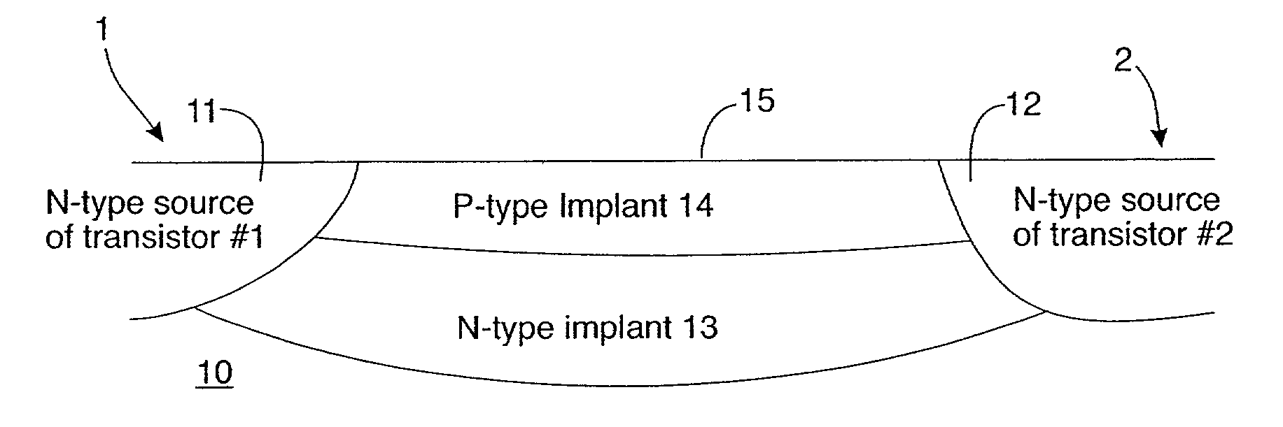
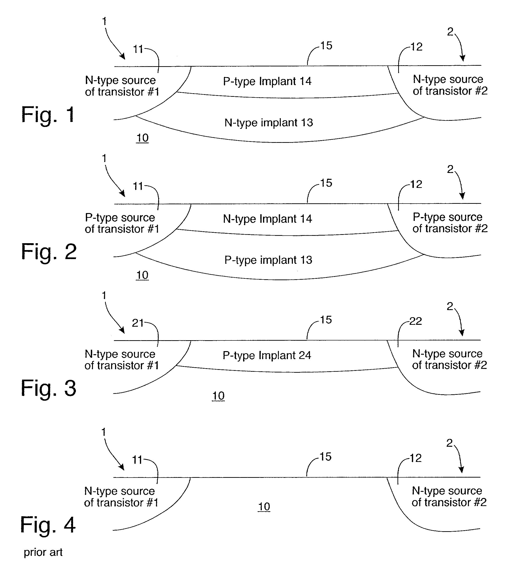
[0015]FIG. 1 is a cross sectional view through a portion of a two interconnected active devices 1, 2 in an integrated circuit. Only a portion of two active devices are shown in FIG. 1 since this invention is concerned with techniques for camouflaging the interconnections rather than with the structure of the devices per se. The depicted portion of active device 1 is a N-type region 11 that could provide the drain, for example, of a first FET transistor 1 and could be formed as an implanted region with a N-type dopant by techniques very well known in the art. Those skilled in the art will recognize, of course, that the N-type region 11 could alternatively form a portion of a diode, a portion of a bipolar transistor or a portion of some other semiconductor structure. The depicted portion of active device 2 is a N-type region 12 that could form the source, for example, of a second FET transistor 2. The function or functions attributed to regions 11 and 12 are not particularly important...
PUM
 Abstract
Description
Claims
Application Information