

Programmable connector/isolator and double polysilicon layer CMOS process with buried contact using the same
a technology of buried contact and cmos, which is applied in the direction of electrical equipment, semiconductor devices, semiconductor/solid-state device details, etc., can solve the problems of unobtrusive and cost-effective fitting, and achieve the effect of preventing reverse engineering of integrated circuits
- Summary
- Abstract
- Description
- Claims
- Application Information
AI Technical Summary
Benefits of technology
Problems solved by technology
Method used
Image

Examples
Embodiment Construction
[0031]Reference will be now made to the drawings where the showings are for the purpose of describing the preferred embodiment of the invention and not for limiting same.
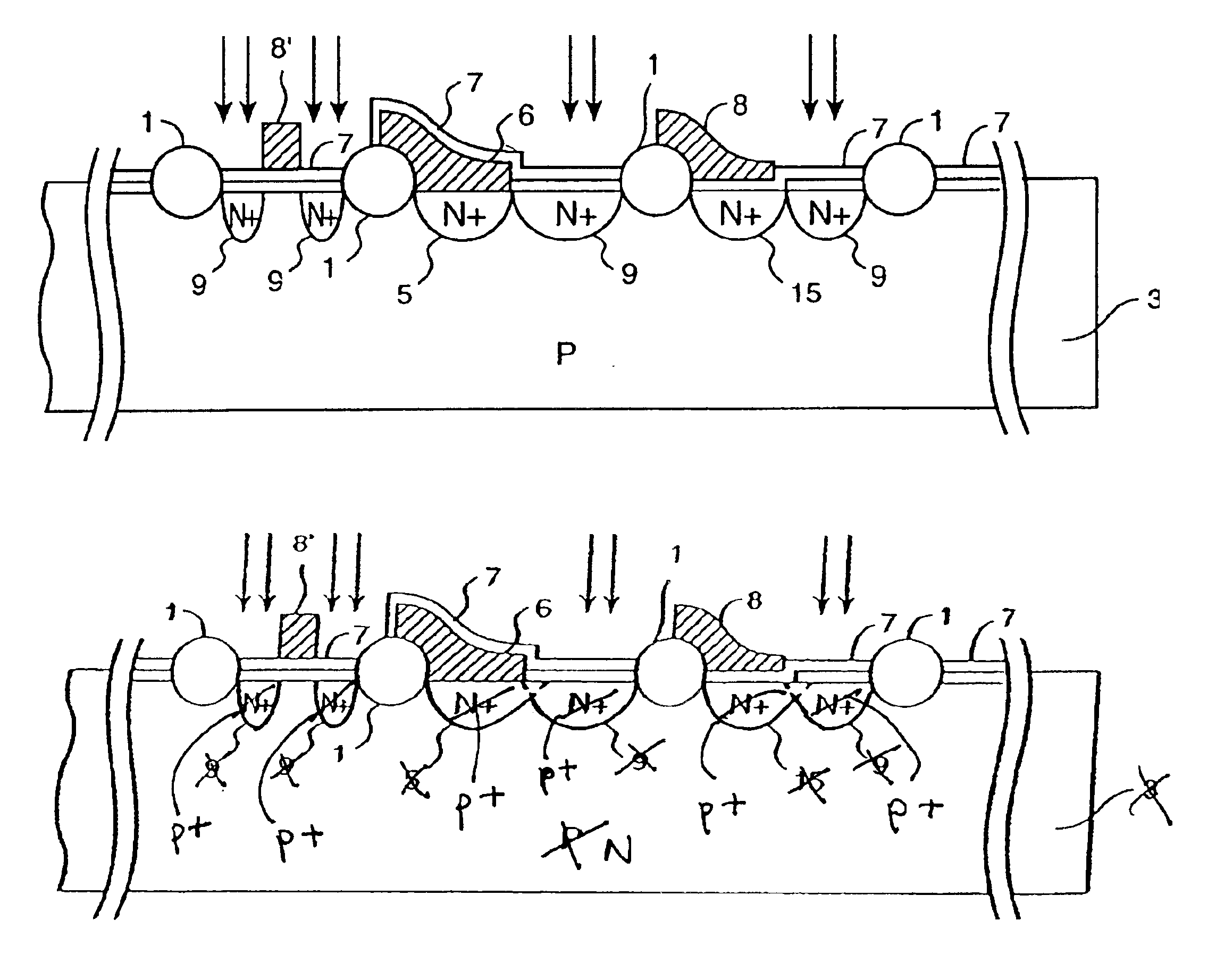
[0032]FIGS. 1 to 7 show the process steps preferably utilized to realize the circuit structure comprising the camouflaged connector / isolator according to the present invention.
[0033]A standard CMOS process proceeds as follows (see also S. M. Sze, supra, p. 447):[0034]1) P-and N-well formation via ion implantation in the substrate;[0035]2) Deposition of the first insulating layer of silicon dioxide and silicon nitride;[0036]3) Patterning for field oxide growth to define active areas; and[0037]4) Growth of the first gate oxide, a thermal oxide of about 100 Å (larger for processes having larger feature sizes).
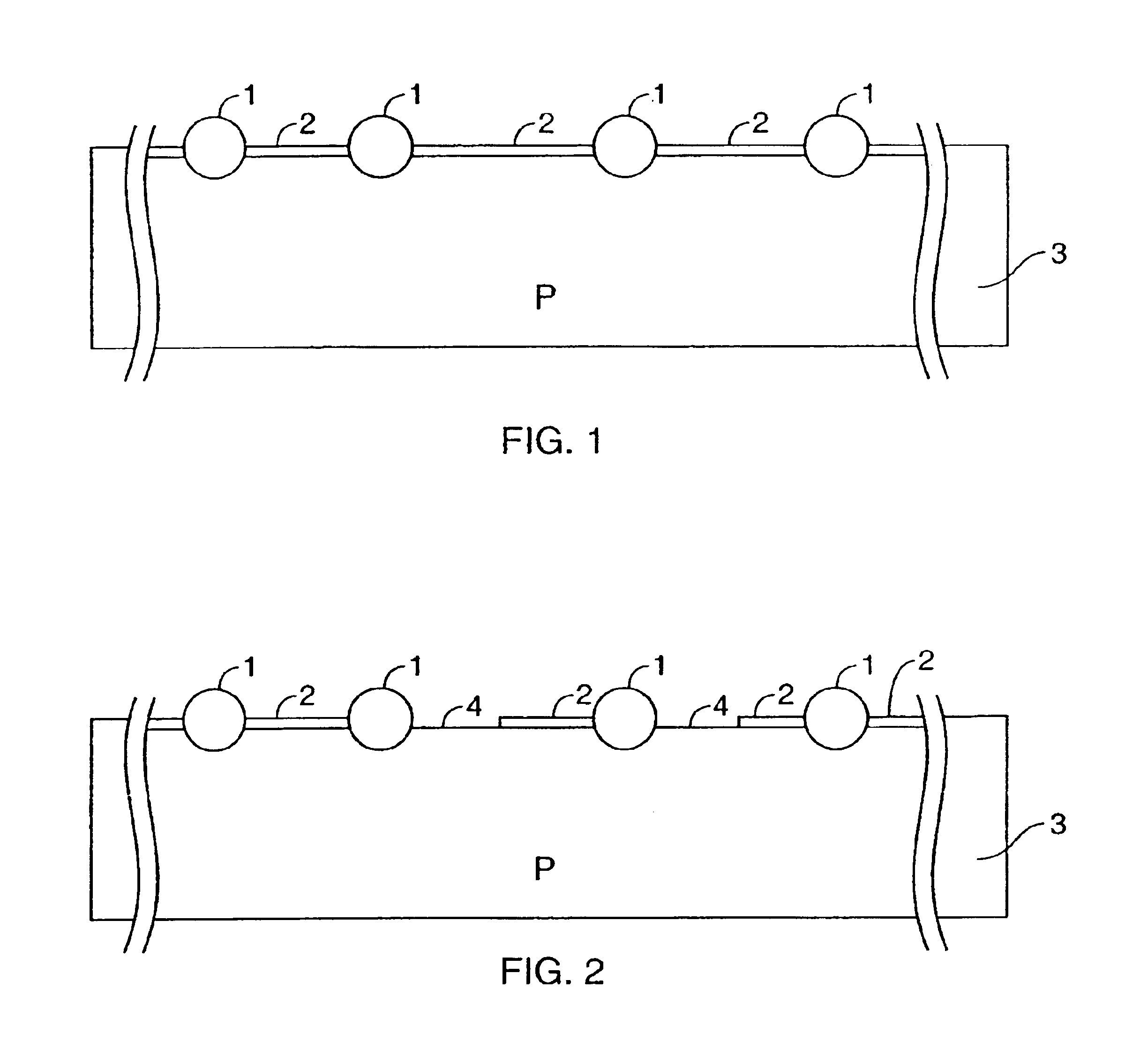
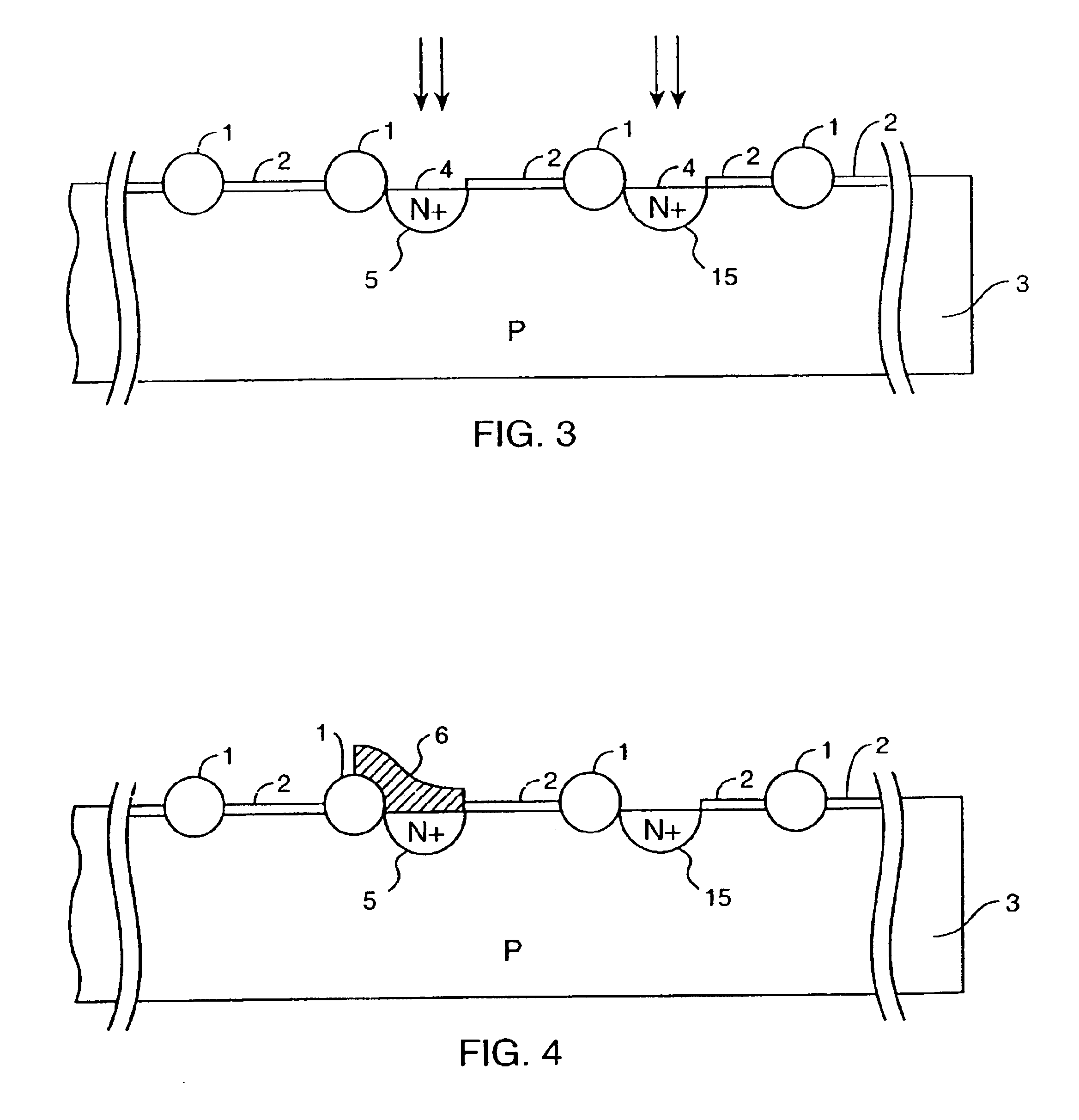
[0038]In this way a structure like the one shown in FIG. 1 is obtained.
[0039]FIG. 1 shows the cross section of the P well portion of a CMOS integrated circuit, processed similarly to the foregoing processes throug...
PUM
 Abstract
Description
Claims
Application Information