
Duty cycle correcting circuits having a variable gain and methods of operating the same

a duty cycle and correcting circuit technology, applied in pulse generators, pulse manipulation, pulse techniques, etc., can solve problems such as circuits that are sensitive to noise, circuits that are not stable, circuits that have a reduced duty cycle correcting range, etc., to reduce the gain responsive to control signals

Inactive Publication Date: 2007-02-20
SAMSUNG ELECTRONICS CO LTD
View PDF13 Cites 62 Cited by
  • Summary
  • Abstract
  • Description
  • Claims
  • Application Information

AI Technical Summary

Benefits of technology

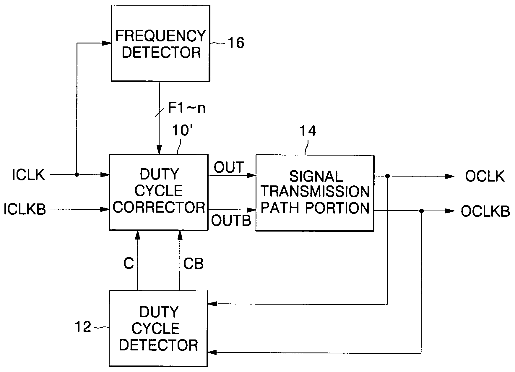
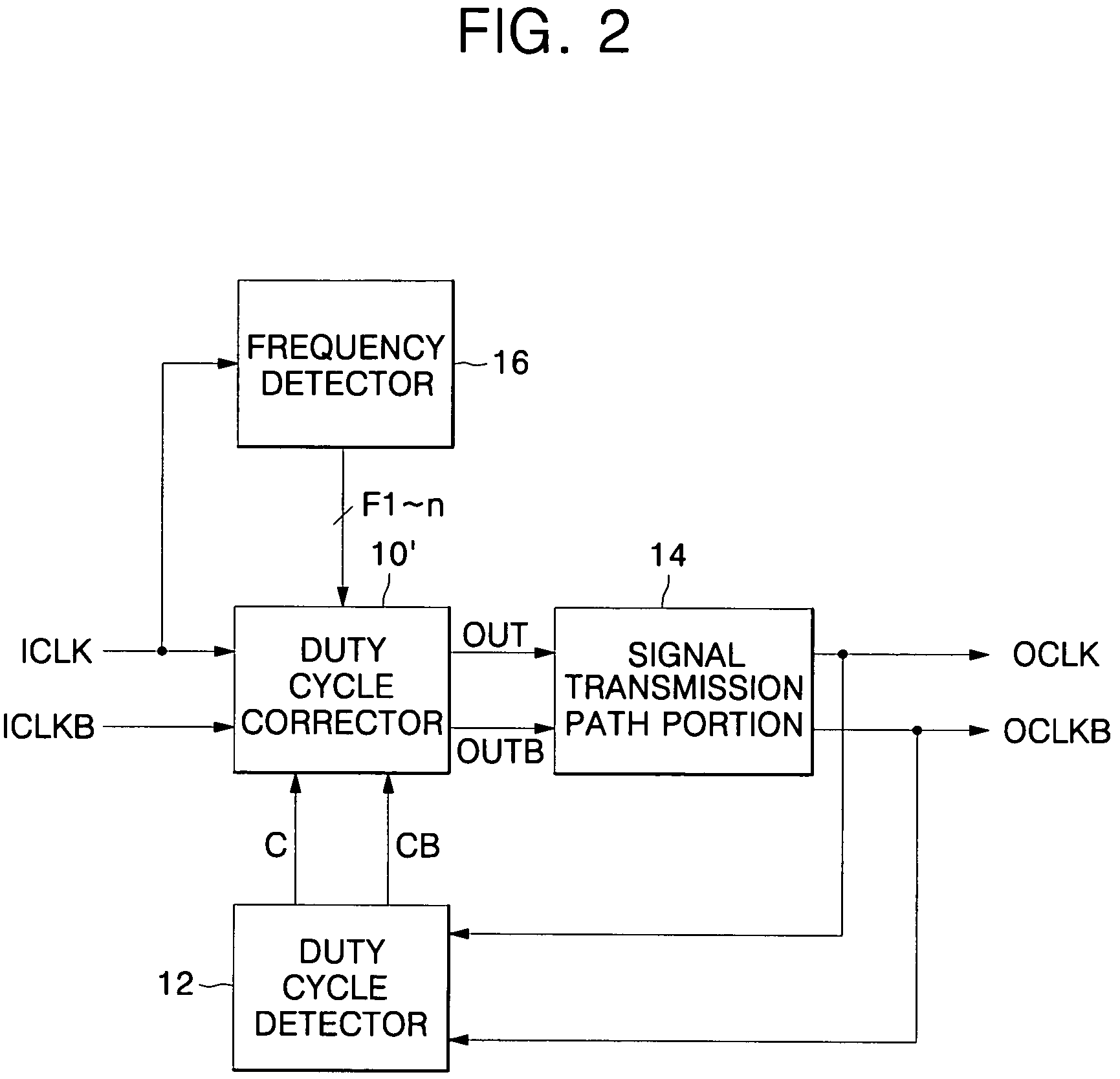
The present invention provides duty cycle correcting circuits and methods that can adjust the gain of a duty cycle correcting circuit based on the frequency of an input clock signal. This allows for automatic adjustment of the gain to ensure optimal performance. The circuits can detect the frequency of the input clock signal and adjust the gain accordingly. Additionally, the circuits can adjust the duty cycle of the output clock signal based on the detected frequency. This results in a corrected clock signal that is more accurate and reliable. The circuits can also include a frequency detecting circuit that selects one of a plurality of gains based on the detected frequency. Overall, the invention provides improved duty cycle correction for clock signals.

Problems solved by technology

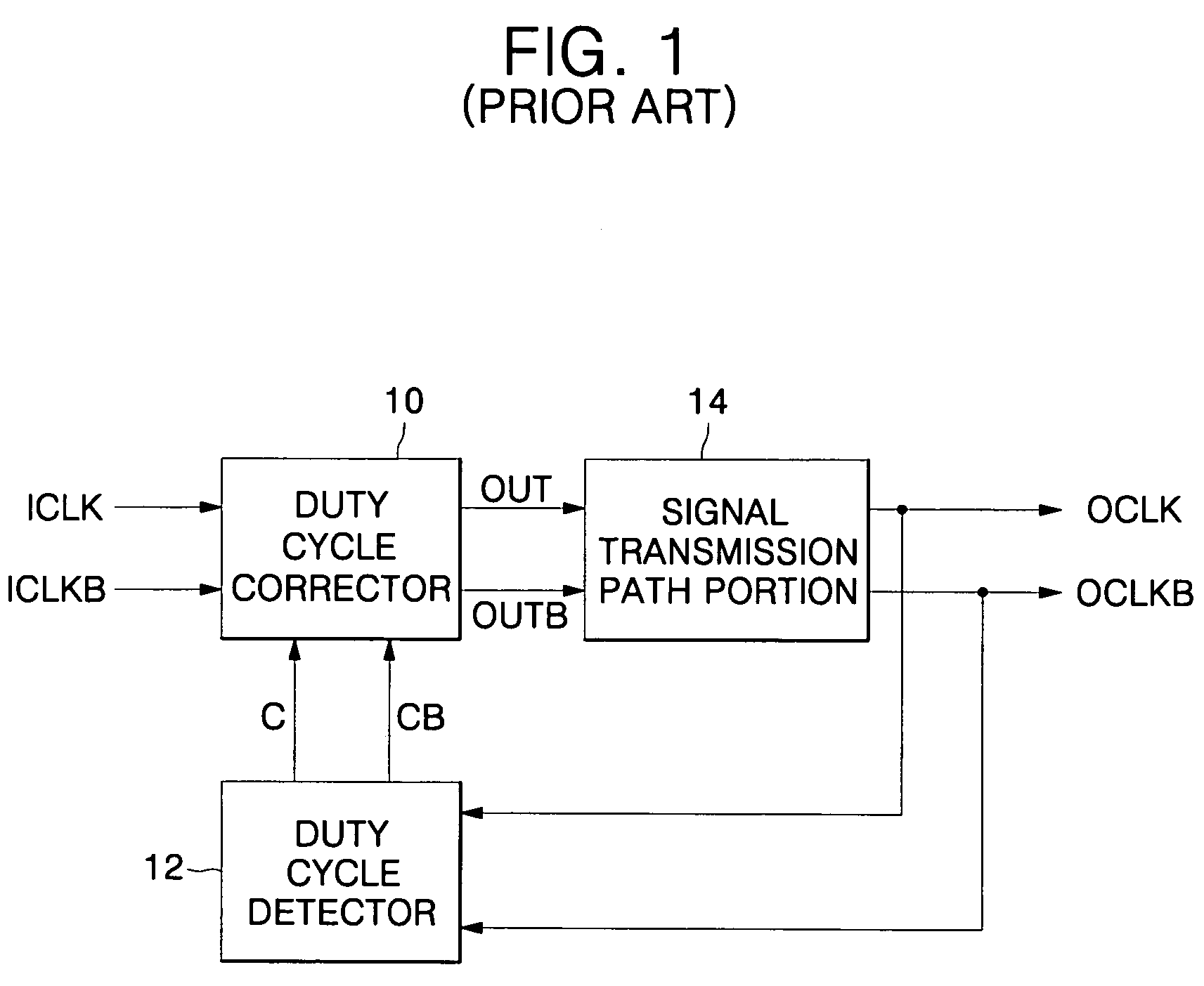
The conventional duty cycle correcting circuit of FIG. 1 may have a problem operating stably with a clock signal having a wide frequency range as its gain is typically fixed.
In other words, if provided a high gain, a conventional circuit like that of FIG. 1 may have an increased duty cycle correcting range for stable operation when a low frequency clock signal is applied but, when a high frequency clock signal is applied, the circuit may become sensitive to noise and may not operate stably.
In contrast, if provided a low gain, the circuit of FIG. 1 may be insensitive to noise and operate stably when a high frequency clock signal is applied but the circuit may have a reduced duty cycle correcting range.
As a result, the circuit may not operate stably when a low frequency clock signal is applied.

Method used


Image

  • Duty cycle correcting circuits having a variable gain and methods of operating the same
  • Duty cycle correcting circuits having a variable gain and methods of operating the same
  • Duty cycle correcting circuits having a variable gain and methods of operating the same

Examples


Embodiment Construction

[0030]The invention is described more fully hereinafter with reference to the accompanying drawings, in which embodiments of the invention are shown. This invention may, however, be embodied in many different forms and should not be construed as limited to the embodiments set forth herein. Rather, these embodiments are provided so that this disclosure will be thorough and complete, and will fully convey the scope of the invention to those skilled in the art. In the drawings, the size and relative sizes of layers and regions may be exaggerated for clarity.

[0031]It will be understood that when an element or layer is referred to as being “on”, “connected to” or “coupled to” another element or layer, it can be directly on, connected or coupled to the other element or layer or intervening elements or layers may be present. In contrast, when an element is referred to as being “directly on,”“directly connected to” or “directly coupled to” another element or layer, there are no intervening ...


PUM


Abstract

Duty cycle correcting circuits having a gain adjusting circuit that selects one of a plurality of gains of the duty cycle correcting circuit based on a frequency of an input signal. An output circuit outputs a duty cycle corrected output signal based on the input signal and the selected one of the plurality of gains. The input signal may be an input clock signal and the output signal may be a corrected clock signal. Methods are also provided.

Description

CROSS-REFERENCE TO RELATED APPLICATION[0001]This application claims the benefit of Korean Patent Application No. 2003-95592, filed Dec. 23, 2003, the disclosure of which is hereby incorporated herein by reference in its entirety.BACKGROUND OF THE INVENTION[0002]The present invention relates to integrated circuit devices and, more particularly, to duty cycle circuits and methods for integrated circuit devices.[0003]It is know for various integrated circuit devices to utilize a duty cycle correcting circuit to adjust the duty cycle of an output clock signal on the integrated circuit device to fifty percent (50%). The duty cycle correcting circuit may include a duty cycle corrector and a duty cycle detector. As used herein, “duty cycle” refers to a ratio of a pulse width with respect to a pulse cycle of a clock signal.[0004]FIG. 1 is a block diagram illustrating a conventional duty cycle correcting circuit. The duty cycle correcting circuit illustrated in FIG. 1 includes a duty cycle c...

Claims


Application Information

Patent Timeline
Patent Type & Authority Patents(United States)
IPC IPC(8): H03K3/017H01L21/82H03K5/15H01L27/00H03K5/04H03K5/156
CPCH03K5/1565H03K5/15
Inventor LEE
Owner SAMSUNG ELECTRONICS CO LTD
Learn More