Flexible circuit board mounted with semiconductor chip and method for mounting semiconductor chip

a flexible circuit board and semiconductor chip technology, applied in the direction of printed circuit non-printed electric components association, printed circuit sustainable manufacturing/processing, final product manufacturing, etc., can solve the problems of insufficient compression, non-uniform terminal pattern of array, and failure to bond neighboring wirings in a stepped portion

Inactive Publication Date: 2007-03-20
TOHOKU PIONEER CORP
View PDF6 Cites 9 Cited by
  • Summary
  • Abstract
  • Description
  • Claims
  • Application Information

AI Technical Summary

Benefits of technology

[0013]The present invention was developed in view of the aforementioned problems, such as with boding the output terminals of a semiconductor chip to a flexible circuit board having a plurality of sections of wirings of different sizes, each section having a pattern of wirings of the same size. It is therefore an object of the present invention to prevent unsuccessful bonding between the wirings and the output terminals. It is another object of the invention to form patterns of wirings corresponding to the semiconductor chip having output terminals of different dimensions to provide interconnection therebetween with high accuracy. It is still another object of the invention to thereby eliminate unevenness in drive currents which would be otherwise caused by variations in resistance across bonding surfaces, thus providing good performance to an electronic appliance, particularly to an organic EL display device whose display performance is directly affected by the magnitude of the drive currents.
[0016]According to a second aspect of the present invention, a method for mounting a semiconductor chip onto a flexible circuit board by electrically connecting predetermined patterns of output terminals of the semiconductor chip to patterns of wirings of the flexible circuit board, the patterns of wirings corresponding to the patterns of output terminals, the method comprising the steps of: providing a flexible circuit board having a plurality of sections of wirings of different sizes formed thereon, each section having a pattern of the wirings of the same size, and a pattern transition region formed between adjacent sections of the wirings of different sizes to prevent unsuccessful interconnection otherwise caused by a difference in size between the wirings; and aligning the patterns of the output terminals with the patterns of the wirings in the wiring sections for electrical interconnection.

Problems solved by technology

In general, the array pattern may often be a non-uniform pattern of terminals, in the case of which the array includes bumps of different dimensions with the bumps of the same dimensions collected in groups, in which the groups are distributed unevenly.
However, employing the conventional wiring pattern forming technique to form such patterns of wirings of different widths would lead to the following problem.
Upon bonding the bumps of the semiconductor chip to the patterned wirings of the flexible circuit board via an anisotropic conductive film by thermo-compression, such a difference in thickness between the patterns of wirings would readily cause unsuccessful bonding of neighboring wirings in a stepped portion.
Effecting a thermo-compression under this condition would cause the pressure to be insufficiently applied to a neighboring portion A around the stepped portion due to the existence of the stepped portion, resulting in an insufficient compression and thus unsuccessful bonding at the neighboring portion A.
However, providing the same thickness to the wirings of different sizes would requires a special processing technique, which could be employed only with extreme difficulties to process such a fine pattern of wirings, thus causing an increase in the manufacturing costs of the flexible circuit board.

Method used


Image

  • Flexible circuit board mounted with semiconductor chip and method for mounting semiconductor chip
  • Flexible circuit board mounted with semiconductor chip and method for mounting semiconductor chip
  • Flexible circuit board mounted with semiconductor chip and method for mounting semiconductor chip

Examples


Embodiment Construction

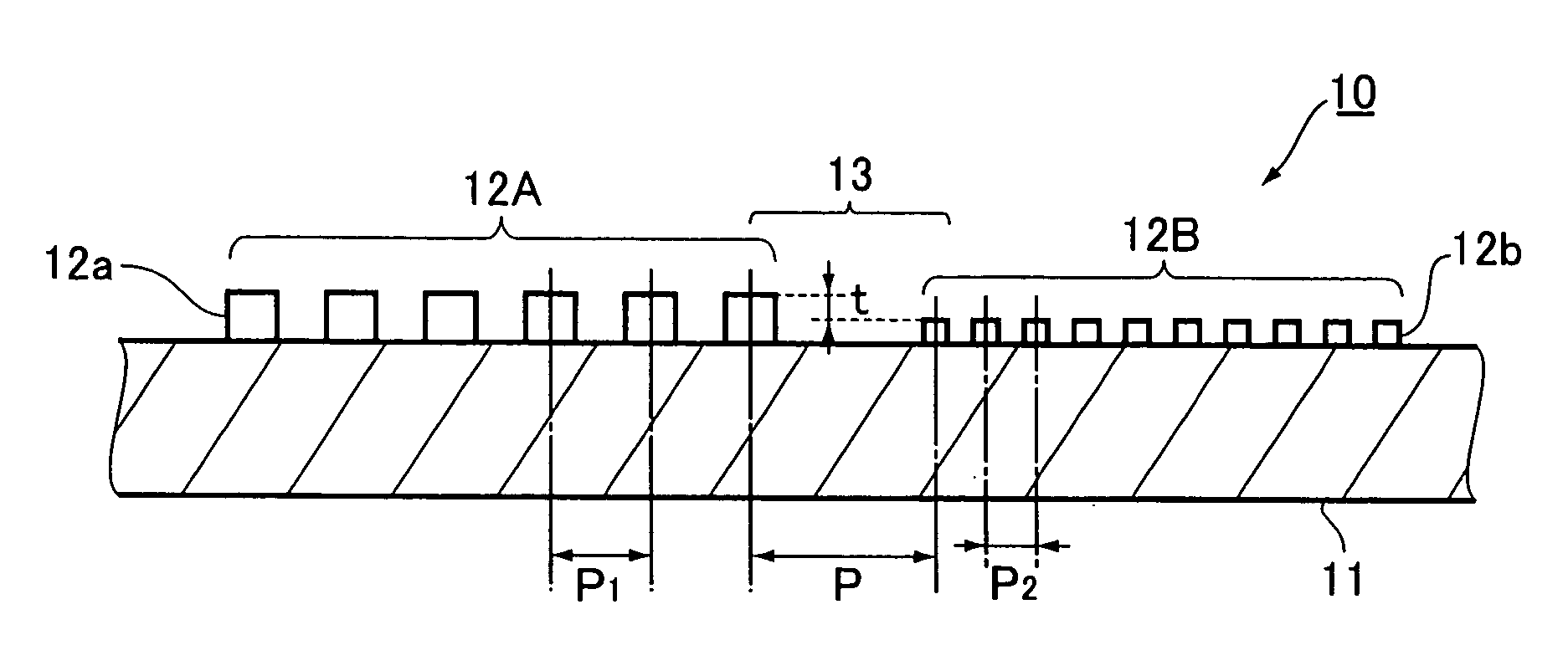
[0027]Now, the present invention will be described below in more detail with reference to the accompanying drawings in accordance with the embodiments. FIG. 3 is an explanatory view illustrating a flexible circuit board according to an embodiment of the present invention. On an insulating material base 11, a flexible circuit board 10 has predetermined patterns of wirings 12a, 12b which are electrically connected to the output terminals of a semiconductor chip. A pattern of the wirings 12a of the same size is formed in a first wiring section 12A, while another pattern of the wirings 12b of the same size is formed in a second wiring section 12B. The present invention is not limited to the two sections 12A, 12B of wirings as shown in the figure, but may also employ a plurality of sections of wirings of different sizes, each section including a pattern of wirings of the same size.

[0028]In the example illustrated, a difference in size between the wirings is a difference in thickness ther...


PUM

PropertyMeasurementUnit
flexibleaaaaaaaaaa
sizesaaaaaaaaaa
sizeaaaaaaaaaa

Abstract

A flexible circuit board is provided to prevent unsuccessful interconnection between the wirings of the flexible circuit board and the output terminals of a semiconductor chip, the flexible circuit board having a plurality of sections of wirings of different sizes, each section including a pattern of wirings of the same size. The flexible circuit board has predetermined patterns of wirings on an insulating material base, and the wirings are electrically connected to the output terminals of a semiconductor chip. A pattern of the wirings of the same size forms a first wiring section, while another pattern of the wirings of the same size form a second wiring section. The flexible circuit board is provided with a pattern transition region between the neighboring wiring sections with wirings of different sizes to avoid unsuccessful interconnection which would be otherwise caused by the difference in size between the wirings.

Description

BACKGROUND OF THE INVENTION[0001]The present invention relates to a flexible circuit board, a flexible circuit board mounted with a semiconductor chip, a display device, and a method for mounting a semiconductor chip.[0002]The present application claims priority from Japanese Patent Application No. 2003-203478, the disclosure of which is incorporated herein by reference.[0003]Electronic appliances, such as mobile phones or PDAs (Personal Digital Assistants or portable information terminals), have been required to have reduced sizes and weights and provide enhanced performance. This in turn requires their electronic components to be more densely incorporated upon the printed circuit board. In particular, thin flat-panel display devices, which are incorporated into such-an electronic appliance to provide as large display screen as possible, require their wired driver components accommodated around the screen to be packed as densely as possible. To meet this requirement, the chip-on-fi...

Claims


Application Information

Patent Timeline
Patent Type & Authority Patents(United States)
IPC IPC(8): H05K1/00H01L21/60H01L23/498H05K1/02H05K1/11H05K1/18H05K3/34
CPCH01L23/4985H05K1/0265H05K1/111H01L24/14H01L24/17H01L23/49822Y10T29/4913H01L2924/12044H05K1/189H05K2201/094H05K2201/09727H05K2201/09736H05K2201/10674H01L2224/16225H01L2224/32225H01L2224/73204H01L23/49838H01L2924/00H01L2924/01322Y02P70/50H05K1/02
Inventor MATSUDA, ATSUSIOHAZAMA, HIDETAKA
Owner TOHOKU PIONEER CORP
Why Eureka
Try Eureka