

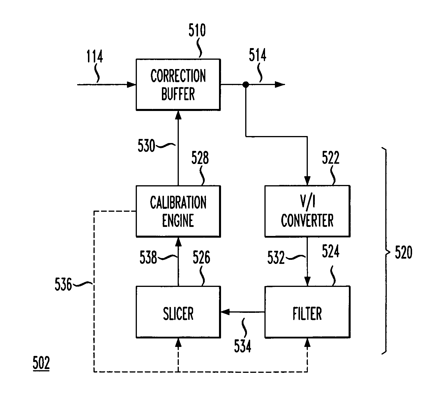
Duty-cycle correction circuit
a duty-cycle correction and circuit technology, applied in the field of electronic devices, can solve the problems that the circuit-fabrication process limitations do not significantly reduce the yield of chips for half-rate clocking systems, and achieve the effect of reducing the yield of chips and reducing the duty-cycle deviation
- Summary
- Abstract
- Description
- Claims
- Application Information
AI Technical Summary
Benefits of technology
Problems solved by technology
Method used
Image

Examples
Embodiment Construction
[0019]Reference herein to “one embodiment” or “an embodiment” means that a particular feature, structure, or characteristic described in connection with the embodiment can be included in at least one embodiment of the invention. The appearances of the phrase “in one embodiment” in various places in the specification are not necessarily all referring to the same embodiment, nor are separate or alternative embodiments mutually exclusive of other embodiments.
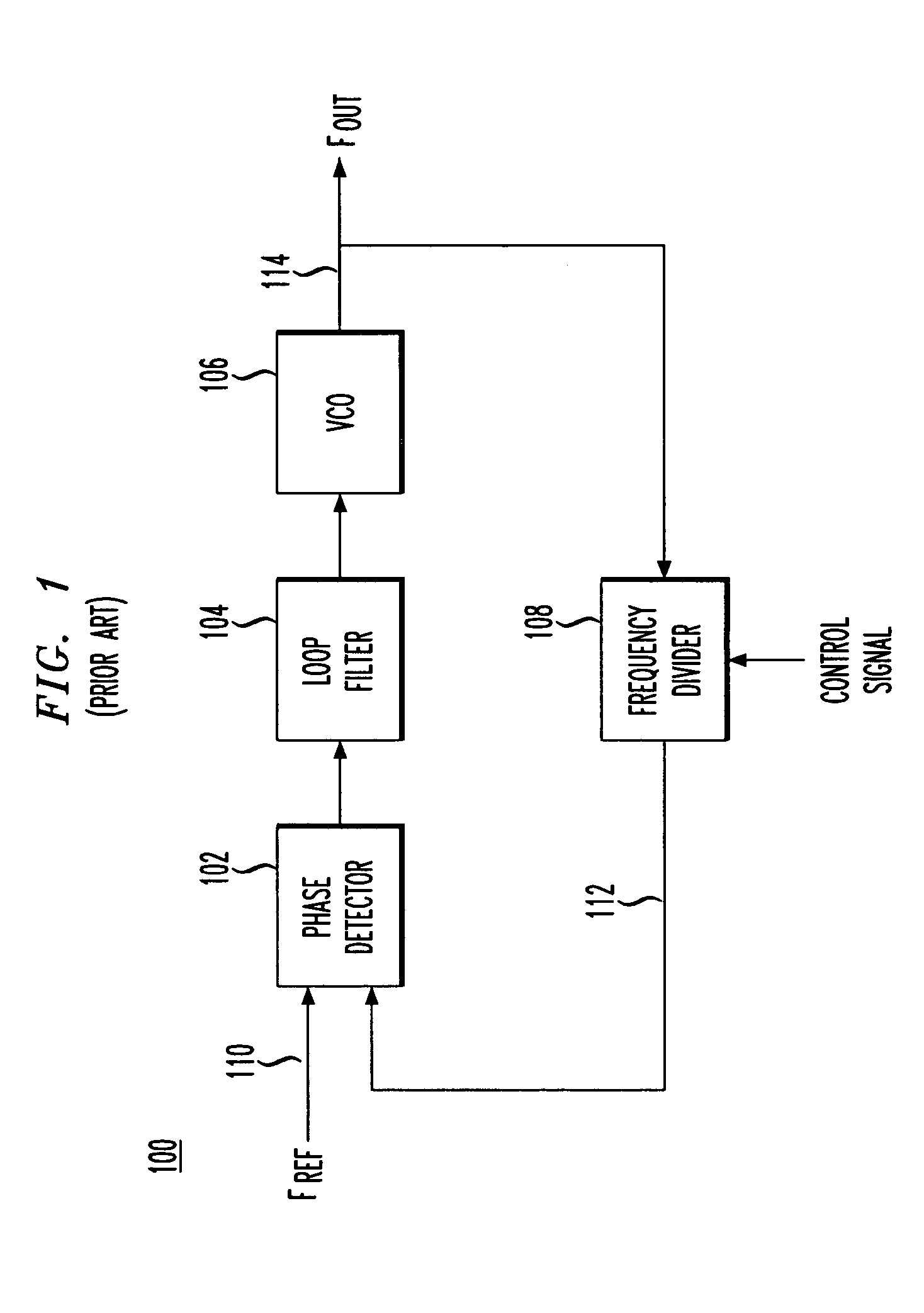
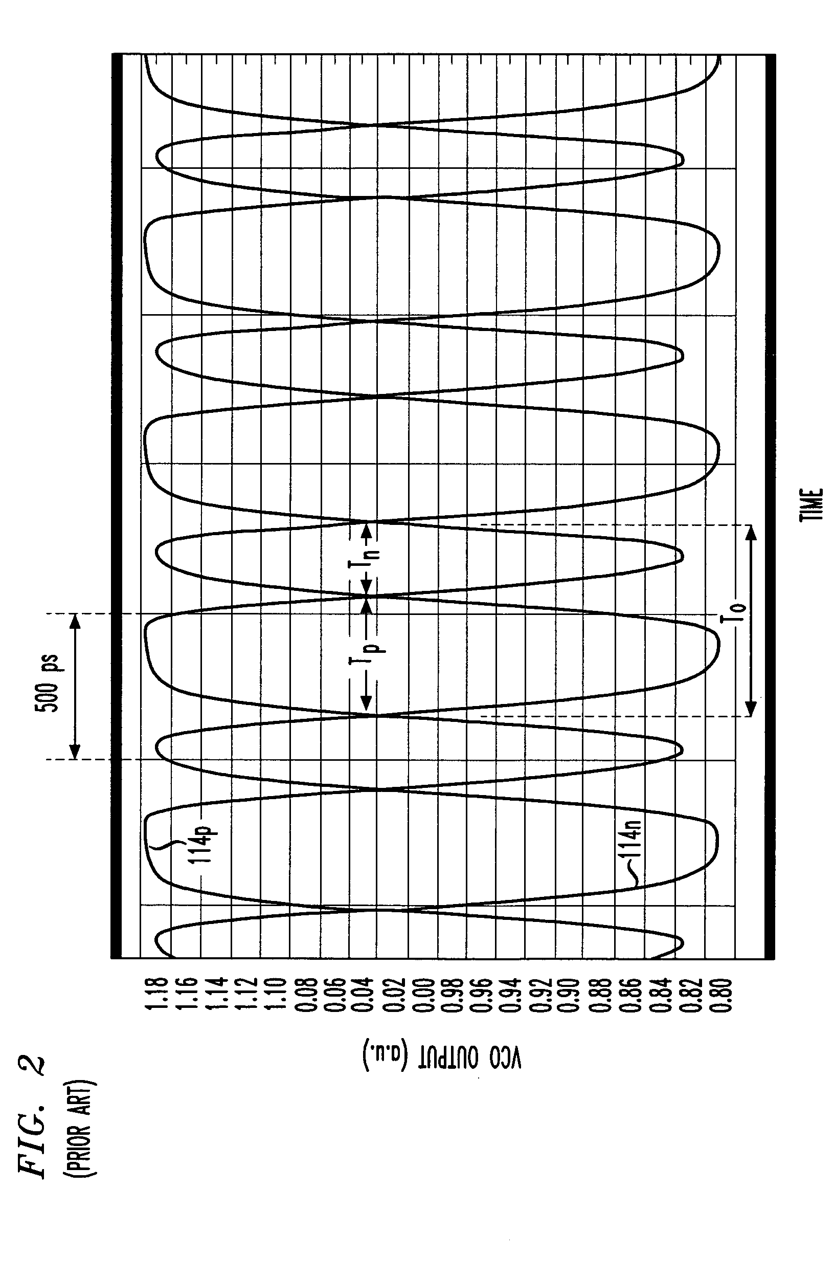
[0020]FIG. 2 graphically shows representative differential output signal 114 of PLL 100 (FIG. 1). Signal 114 is characterized by a period T0 and has two components 114p and 114n. Within each cycle of signal 114, signal 114p is greater than signal 114n for a time interval Tp, and signal 114n is greater than signal 114p for a time interval Tn, where Tp+Tn=T0. The duty cycle of signal 114 is determined, e.g., by the value of Tp / T0, and is 50% when Tp / T0=Tn / T0=0.5. In signal 114 shown in FIG. 2, the duty cycle is about 62% and the devi...
PUM
 Abstract
Description
Claims
Application Information