Land grid array packaged device and method of forming same

a technology of integrated circuits and packaged devices, which is applied in the direction of semiconductor devices, semiconductor/solid-state device details, electrical equipment, etc., can solve the problems of time-consuming and expensive leadframe formation and packaging of devices

Inactive Publication Date: 2007-04-17
TAIWAN SEMICON MFG CO LTD
View PDF11 Cites 69 Cited by
  • Summary
  • Abstract
  • Description
  • Claims
  • Application Information

AI Technical Summary

Problems solved by technology

However, it can be expensive and time-consuming to form a leadframe and package a device if steps like chemical etching and etch back are required.

Method used


Image

  • Land grid array packaged device and method of forming same
  • Land grid array packaged device and method of forming same
  • Land grid array packaged device and method of forming same

Examples


Embodiment Construction

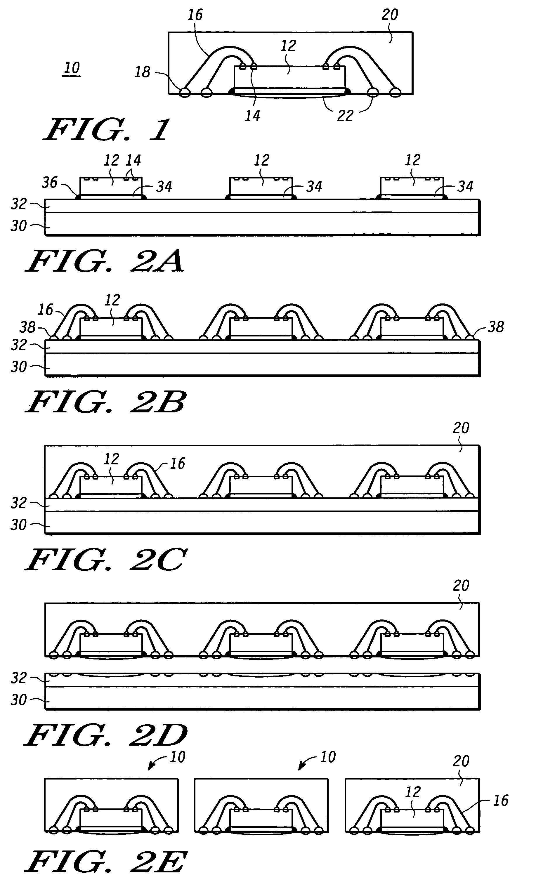
[0011]The detailed description set forth below in connection with the appended drawings is intended as a description of the presently preferred embodiments of the invention, and is not intended to represent the only form in which the present invention may be practiced. It is to be understood that the same or equivalent functions may be accomplished by different embodiments that are intended to be encompassed within the spirit and scope of the invention.

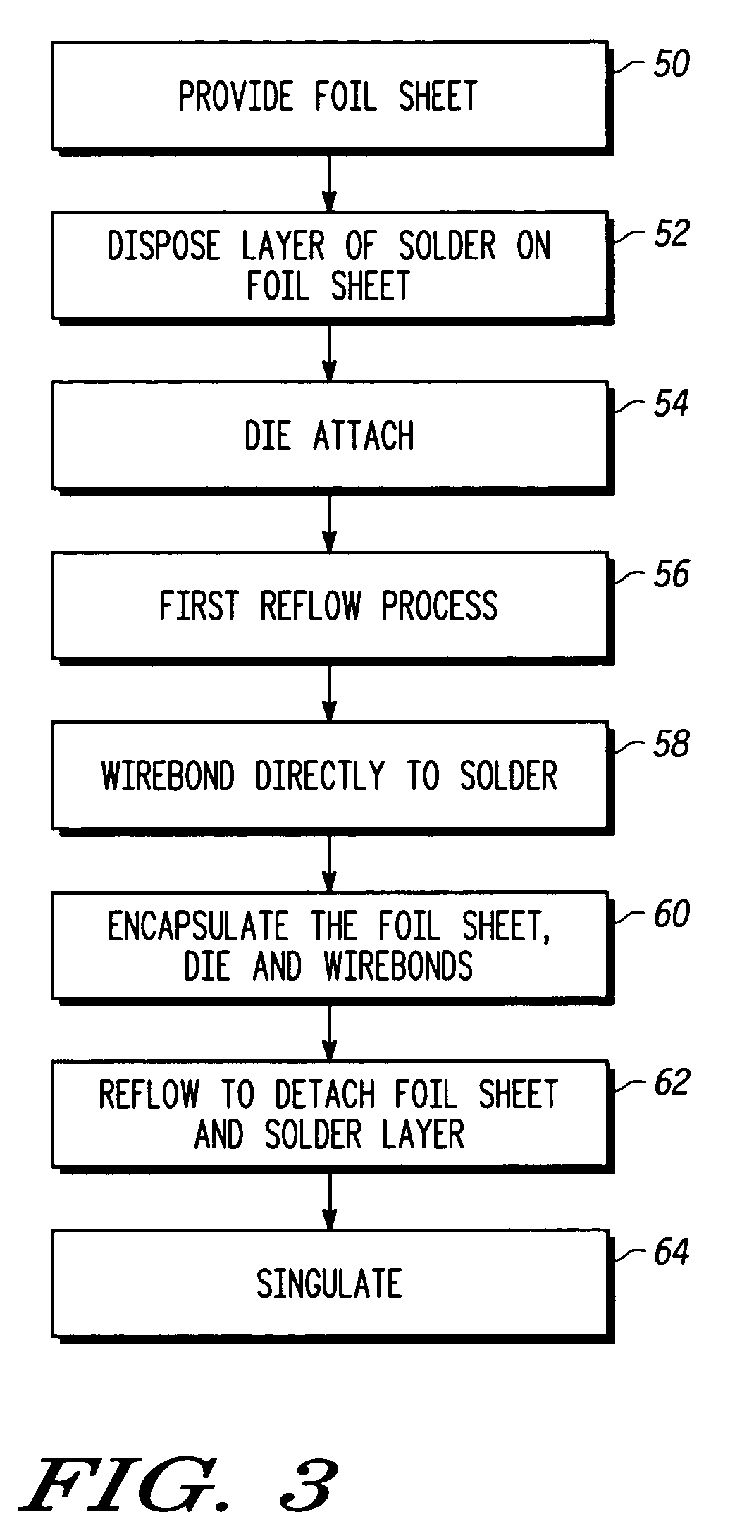
[0012]The present invention provides a method of packaging an integrated circuit die, including the steps of:

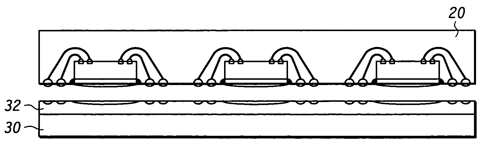
[0013]providing a foil sheet;

[0014]forming a layer of solder on a first side of the foil sheet;

[0015]attaching a first side of an integrated circuit die to the solder on the foil sheet, wherein the first side of the die includes a layer of metal thereon and a second, opposing side of the die includes a plurality of bonding pads;

[0016]electrically connecting the bonding pads to the solder on the foil sheet with a plurality of wi...


PUM


Abstract

A method of packaging an integrated circuit die (12) includes the steps of providing a foil sheet (30) and forming a layer of solder (32) on a first side of the foil sheet. A first side of the integrated circuit die is attached to the solder on the foil sheet. The first side of the die has a layer of metal (34) on it and a second, opposing side of the die includes bonding pads (14). The bonding pads are electrically connected to the solder on the foil sheet with wires (16). The die, the electrical connections, and the first side of the foil sheet are encapsulated with a mold compound (20). The foil sheet is separated from the die and the wires, which forms a packaged integrated circuit (10).

Description

BACKGROUND OF THE INVENTION[0001]The present invention relates to integrated circuit packaging, and more particularly to an improved process for fabricating a Land Grid Array (LGA) packaged device.[0002]An integrated circuit (IC) die is a small device formed on a semiconductor wafer, such as a silicon wafer. A leadframe is a metal frame that usually includes a paddle that supports the IC die that has been cut from the wafer. The leadframe also has lead fingers that provide external electrical connections. That is, the die is attached to the die paddle and then bonding pads of the die are connected to the lead fingers via wire bonding or flip chip bumping to provide the external electrical connections. Encapsulating the die and wire bonds or flip chip bumps with a protective material forms a package. Depending on the package type, the external electrical connections may be used as-is, such as in a Thin Small Outline Package (TSOP), or further processed, such as by attaching spherical...

Claims


Application Information

Patent Timeline
Patent Type & Authority Patents(United States)
IPC IPC(8): H01L21/00H01L21/44H01L21/56H01L23/31
CPCH01L21/56H01L23/3107H01L21/568H01L24/97H01L2224/92247H01L2224/48091H01L2224/48137H01L2924/01079H01L2924/14H01L2224/73265H01L2924/10253H01L24/48H01L2924/00014H01L2924/00H01L2924/181H01L2924/18165H01L2924/00012H01L2224/45099H01L2224/45015H01L2924/207H01L21/44
Inventor SHIU, HEI MINGLEE, KAM FAIWONG, HO WANG
Owner TAIWAN SEMICON MFG CO LTD
Why Eureka
Try Eureka