Zero-bias-power level shifting

a technology of bias power level and voltage translation, applied in logic circuits, pulse automatic control, reliability increasing modifications, etc., can solve problems such as leakage current, undesirable current associated with manufacturing processes, and the destruction of low-voltage transistors

Active Publication Date: 2007-04-17
VIA TECH INC
View PDF11 Cites 21 Cited by
  • Summary
  • Abstract
  • Description
  • Claims
  • Application Information

AI Technical Summary

Problems solved by technology

The lower voltage transistors could be destroyed if they are exposed to the higher voltage range.
“Bias current” is an undesirable but necessary current associated with a circuit structure and is often independent of manufacturing process.
“Leakage current,” on the other hand, is an undesirable current associated with a manufacturing process.
Generally leakage current cannot be eliminated through circuit techniques.
A problem with this circuit is that since Dvdd and Avdd are from different voltage sources, they are usually derived from different circuitry.
Although the 1.2V-gate-driven n-channel transistor can be sized to compensate for a 3.3V-gate-driven p-channel transistor under typical conditions, the compensation may not be maintained as operating and manufacturing conditions vary.
Furthermore, as variations from typical conditions arise, n-channel transistor and p-channel transistor mismatches introduce signal distortion due to unmatched rising and falling propagation delays.
Whereas the signal integrity features of the circuit of FIG. 1B are an improvement from those of the circuit in FIG. 1A, the steady-state bias current makes the circuit of FIG. 1B undesirable for low-power applications.
Thus, a heretofore unaddressed need exists in the industry to address the aforementioned deficiencies and inadequacies.

Method used


Image

  • Zero-bias-power level shifting
  • Zero-bias-power level shifting
  • Zero-bias-power level shifting

Examples


Embodiment Construction

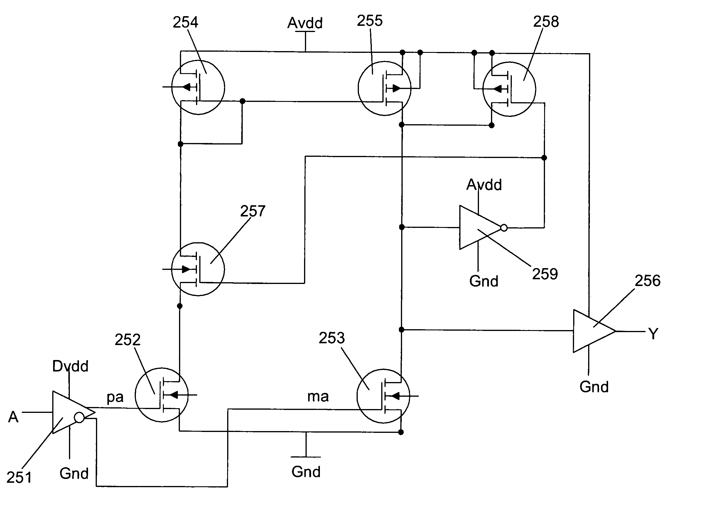
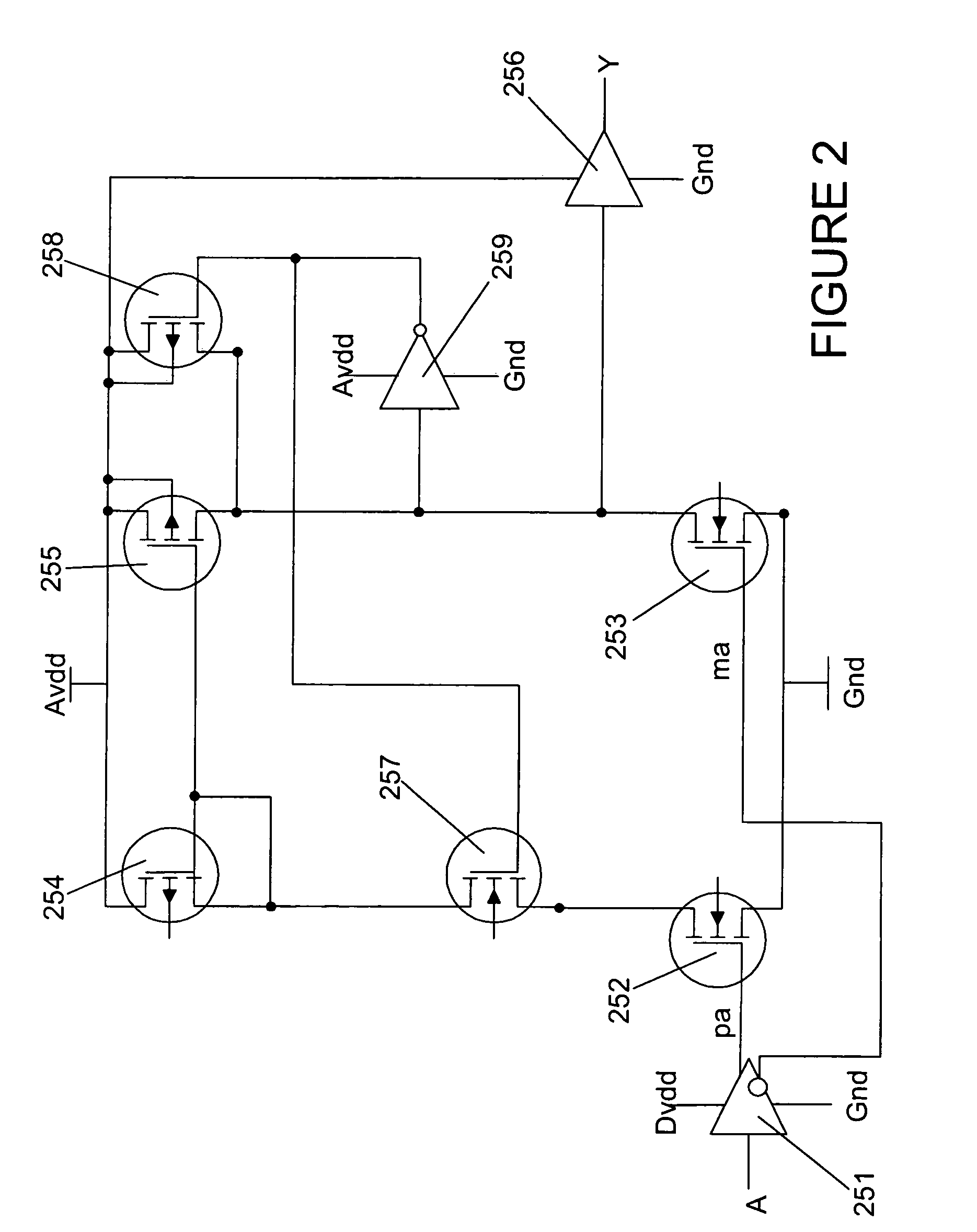
[0030]Disclosed herein are systems and methods for voltage level shifting with zero bias current. To facilitate description of the inventive systems, an example system that can be used to implement the systems and methods for voltage level shifting with zero bias current is discussed with reference to the figures. Although this system is described in detail, it will be appreciated that this system is provided for purposes of illustration only and modifications are feasible without departing from the inventive concept.

[0031]Referring now and in more detail to the drawings in which like numerals indicate corresponding parts through the several views, this disclosure describes a zero bias power voltage level shifting system. It details how the system is configured and how it operates. Of course, a variety of alternative embodiments and implementations will be appreciated from the exemplary embodiment described herein, consistent with the scope and spirit of the present invention.

[0032]...


PUM


Abstract

A circuit for voltage level translation with zero static current is disclosed for interfacing devices at one supply voltage with devices at another supply voltage. The translation is achieved by using a modified current mirror circuit such that the current mirror is effectively turned off when the output reaches a steady state condition.

Description

TECHNICAL FIELD[0001]The present invention is generally related to electronic circuits and, more particularly, is related to a system and method of voltage translation.BACKGROUND OF THE INVENTION[0002]Many electronics systems use multiple voltage supplies to power semiconductor devices. To enable a device powered at one voltage level to interface with a device powered at a second voltage level, it is often desirable to use a circuit to shift between the voltage levels.[0003]Two common level shifting techniques used today are shown in FIGS. 1A and 1B. The circuits provided and herein are illustrated with MOSFETs for the sake of simplicity. However, one of ordinary skill in the art would appreciate that other types of transistors would work in these circuits and that there are trade-offs associated with using the other types of transistors. FIG. 1A involves an n-channel input circuit and a cross coupled p-channel circuit. The p-channel circuit 104, 105 and buffer 106 operate within a ...

Claims


Application Information

Patent Timeline
Patent Type & Authority Patents(United States)
IPC IPC(8): H03L5/00
CPCH03K19/0016H03K19/00323
Inventor DAVIS, TIMOTHY
Owner VIA TECH INC
Why Eureka
Try Eureka