
Hybrid integrated circuit device and method of manufacturing the same

a hybrid integrated circuit and integrated circuit technology, applied in the direction of printed circuit aspects, non-metallic protective coating applications, printed electric component incorporation, etc., can solve the problems of large device, inability to increase the density of hybrid integrated circuits, and inability to separate circuit boards easily, so as to suppress shorts of electric circuits and achieve easy separation of circuit boards

Active Publication Date: 2007-06-19
SEMICON COMPONENTS IND LLC
View PDF8 Cites 20 Cited by
  • Summary
  • Abstract
  • Description
  • Claims
  • Application Information

AI Technical Summary

Benefits of technology

[0028]In the method of manufacturing the hybrid integrated circuit device according to this aspect, first, the first and second grooves are formed, and the hybrid integrated circuits are integrated on the surfaces of the respective circuit boards. Thereafter, the individual circuit boards are separated from the others. In this way, the separation of the circuit boards can be easily performed. Moreover, since conductive dust produced upon this separation can be caused to occur as scarcely as possible, it is possible to suppress a short of an electric circuit due to the dust.

Problems solved by technology

However, the above-described hybrid integrated circuit device and method of manufacturing the same have had problems as described below.
Accordingly, the peripheral portions of the circuit boards 60 are dead spaces, and therefore, there has been a problem that an entire device becomes large even if the degree of integration of the hybrid integrated circuit 67 is increased.
This fact becomes a constraint when the conductive patterns 62 are designed, and therefore, there has been a problem that the density of the hybrid integrated circuit cannot be increased.
Moreover, since the side surface portions of the board are vertically formed, there has been a problem that when the board is sealed with resin, the adhesion between the board and the sealing resin is poor.
Accordingly, there has been a problem that a blade of a press for performing “punching” is worn out soon.
Moreover, the replacement of a blade of a press is work requiring skilled labor, and what is more, takes a very long time.
Therefore, there has been a problem that the productivity is reduced.
In addition, this blade used for punching is very expensive.
Therefore, further, the fact that the life of this blade is very short may cause an increase in the cost of an entire device.
Accordingly, there has been a problem that the loss from disposal of the metal board 66B, which is a material, becomes large.

Method used


Image

  • Hybrid integrated circuit device and method of manufacturing the same
  • Hybrid integrated circuit device and method of manufacturing the same
  • Hybrid integrated circuit device and method of manufacturing the same

Examples


second embodiment

(Second Embodiment for Describing Method of Manufacturing Hybrid Integrated Circuit Device)

[0068]A description will be given of a method of manufacturing the hybrid integrated circuit device described in the first embodiment, with reference to FIGS. 3A to 10.

[0069]First Process (see FIGS. 3A to 3C)

[0070]This process is a process of forming an intermediate metal board 10B by splitting a large metal board 10A.

[0071]First, referring to FIG. 3A, the large metal board 10A is prepared. The size of the large metal board 10A is, for example, approximately one meter square. Here, the metal board 10A is an aluminum board with both faces anodized. An insulating layer is provided on the surface of the metal board 10A. Moreover, copper foil to become conductive patterns is formed on the surface of the insulating layer. In addition, in the case of forming multi-layer conductive patterns, multiple sheets of copper foil are attached with an insulating layer interposed between each of the sheets of ...


PUM


Abstract

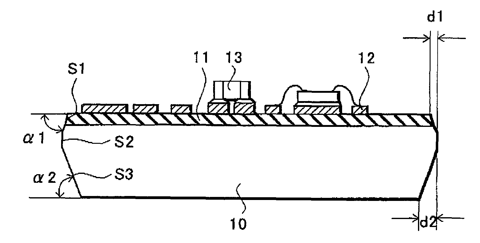
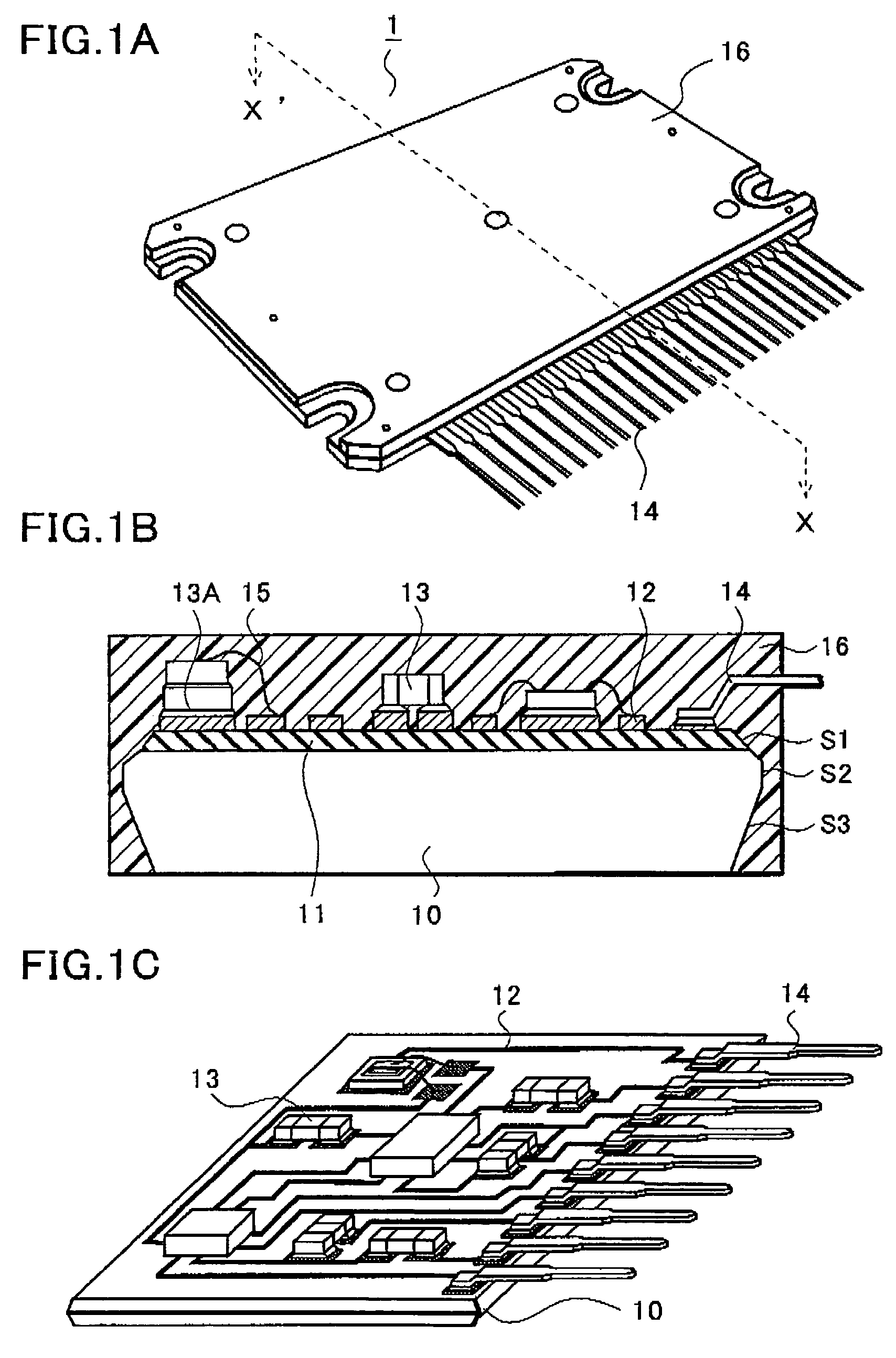
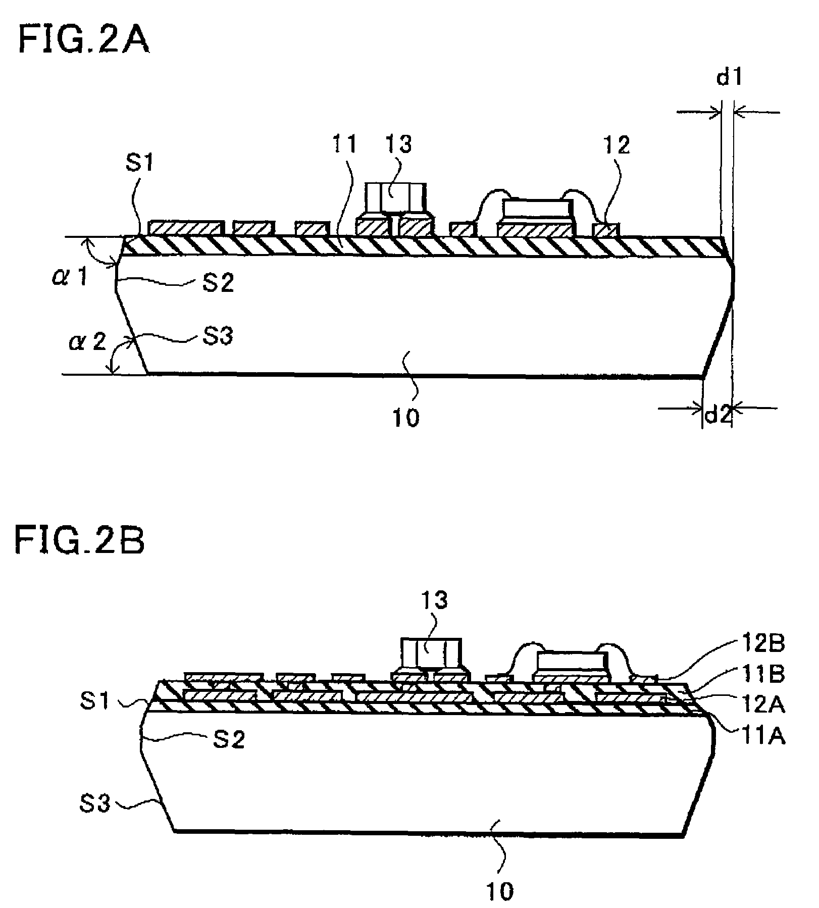
An object of the present invention is to provide a method of manufacturing a hybrid integrated circuit device, in which multiple circuit boards are manufactured from one large metal board by dicing. The hybrid integrated circuit device of the present invention includes a circuit board with a surface provided with an insulating layer, and conductive patterns provided on the insulating layer. Circuit elements are electrically connected to the conductive patterns. Further, each side surface of the circuit board includes a first inclined portion extending obliquely downward from a peripheral portion of the surface of the circuit board, and a second inclined portion extending obliquely upward from a back surface of the circuit board and formed to be larger than the first inclined portion.

Description

BACKGROUND OF THE INVENTION[0001]Priority is claimed to Japanese Patent Application Number JP2003-333888 filed on Sep. 25, 2003, the disclosure of which is incorporated herein by reference in its entirety.[0002]1. Field of the Invention[0003]The present invention relates to a hybrid integrated circuit device and a method of manufacturing the same. The present invention particularly relates to a hybrid integrated circuit device obtained by manufacturing multiple circuit boards from one large metal board, and a method of manufacturing the hybrid integrated circuit device.[0004]2. Description of the Related Art[0005]A description will be given of a constitution of a conventional hybrid integrated circuit device with reference to FIGS. 11A and 11B. FIG. 11A is a perspective view of a hybrid integrated circuit device 6, and FIG. 11B is a sectional view taken along the line X–X′ in FIG. 11A.[0006]Referring to FIGS. 11A and 11B, the conventional hybrid integrated circuit device 6 has a con...

Claims


Application Information

Patent Timeline
Patent Type & Authority Patents(United States)
IPC IPC(8): H05K1/16H05K1/02H01L21/84H01L23/13H01L25/16H01L27/12H05K1/00H05K1/05H05K3/00H05K3/28H05K3/46H05K7/02
CPCH01L21/565H01L21/84H01L23/13H01L24/97H01L27/12H05K3/0052H01L25/16H01L2224/48091H01L2224/73265H01L2224/97H01L2924/01013H01L2924/01029H01L2924/01033H01L2924/01082H01L2924/14H01L2924/19041H01L2924/19042H01L2924/19043H01L2924/19105H01L2924/30107H05K1/056H05K3/284H05K2201/09036H05K2201/0909H05K2201/09827H05K2203/1572H01L2224/85H01L2924/00014H01L2224/83H01L24/48H01L2924/01005H01L2924/01006H01L2924/01023H01L2224/32225H01L2224/451H01L2924/12042H01L24/45H01L2924/181H01L2924/00015H01L2224/05599H01L2924/00H01L2924/00012H05K1/02
Inventor MIZUTANI, MASAHIKONOGUCHI, MITSURUTAKAKUSAKI, NOBUHISA
Owner SEMICON COMPONENTS IND LLC
Learn More