Method for detaching a semiconductor chip from a foil and device for mounting semiconductor chips

a technology for semiconductor chips and foils, which is applied in the direction of coin-freed apparatus, lighting and heating apparatus, instruments, etc., can solve the problems of damage to adjacent semiconductor chips, and achieve the effect of reducing the contact area between the foil and the semiconductor chip, reducing the adhesion of the semiconductor chip to the foil, and easy picking up

Inactive Publication Date: 2007-07-03
ESEC
View PDF8 Cites 33 Cited by
  • Summary
  • Abstract
  • Description
  • Claims
  • Application Information

AI Technical Summary

Benefits of technology

[0015]With this procedure step, the foil is pulled over the stripping edge of the ramp. The semiconductor chip is moved with it. In doing so, the foil detaches itself from the underneath of the semiconductor chip. The part of the semiconductor chip detached from the foil hangs at an angle in the air like a plate supported on only one side. When the rear end of the semiconductor chip reaches the stripping edge of the ramp, then the semiconductor chip falls back onto the foil. The semiconductor chip however, is now located above the support area where the foil is pulled into the grooves of the support area. The adhesion of the semiconductor chip to the foil is therefore greatly reduced.
[0022]The method for picking a thin semiconductor chip from a foil is therefore characterised in that the detachment of the semiconductor chip from the foil and the picking of the semiconductor chip by a chip gripper takes place in two from each other independent, successive procedure steps. After detachment, the semiconductor chip again lands on the foil. However, because the greater part of the foil is pulled into the grooves in the support area, the contact area between the foil and the semiconductor chip is significantly reduced. Correspondingly, the adhesion of the semiconductor chip to the foil is also reduced and the semiconductor chip can easily be picked up by the chip gripper.
[0023]Preferably, ultrasound can be applied to the ramp with the stripping edge so that the detachment process can be supported by ultrasound. Furthermore, it is advantageous when the height of the stripping edge is adjustable so that the height can be reduced immediately before the semiconductor chip is completely detached from the foil.
[0025]Because, with typically 0.3 millimeters, and at most 0.4 millimeters, the height difference at the stripping edge of the ramp is very small, therefore adjacent semiconductor chips are not damaged even when their edge is also moved over the ramp.

Problems solved by technology

On the other hand, in order to additionally reduce the adhesion of the semiconductor chips to the foil, the foil is heated to a temperature of 50° C. to 65° C. This method works for numerous semiconductor chips however, with comparatively large but very thin semiconductor chips, it often happens that, on applying the vacuum and removing the foil, the semiconductor chips lift and then fall back onto the foil whereby it can also happen that adjacent semiconductor chips overlap.
These methods have the disadvantage that adjacent semiconductor chips can be damaged because the height of the edge necessary for detachment has to be about 1.5 millimeters.

Method used


Image

  • Method for detaching a semiconductor chip from a foil and device for mounting semiconductor chips
  • Method for detaching a semiconductor chip from a foil and device for mounting semiconductor chips
  • Method for detaching a semiconductor chip from a foil and device for mounting semiconductor chips

Examples


Embodiment Construction

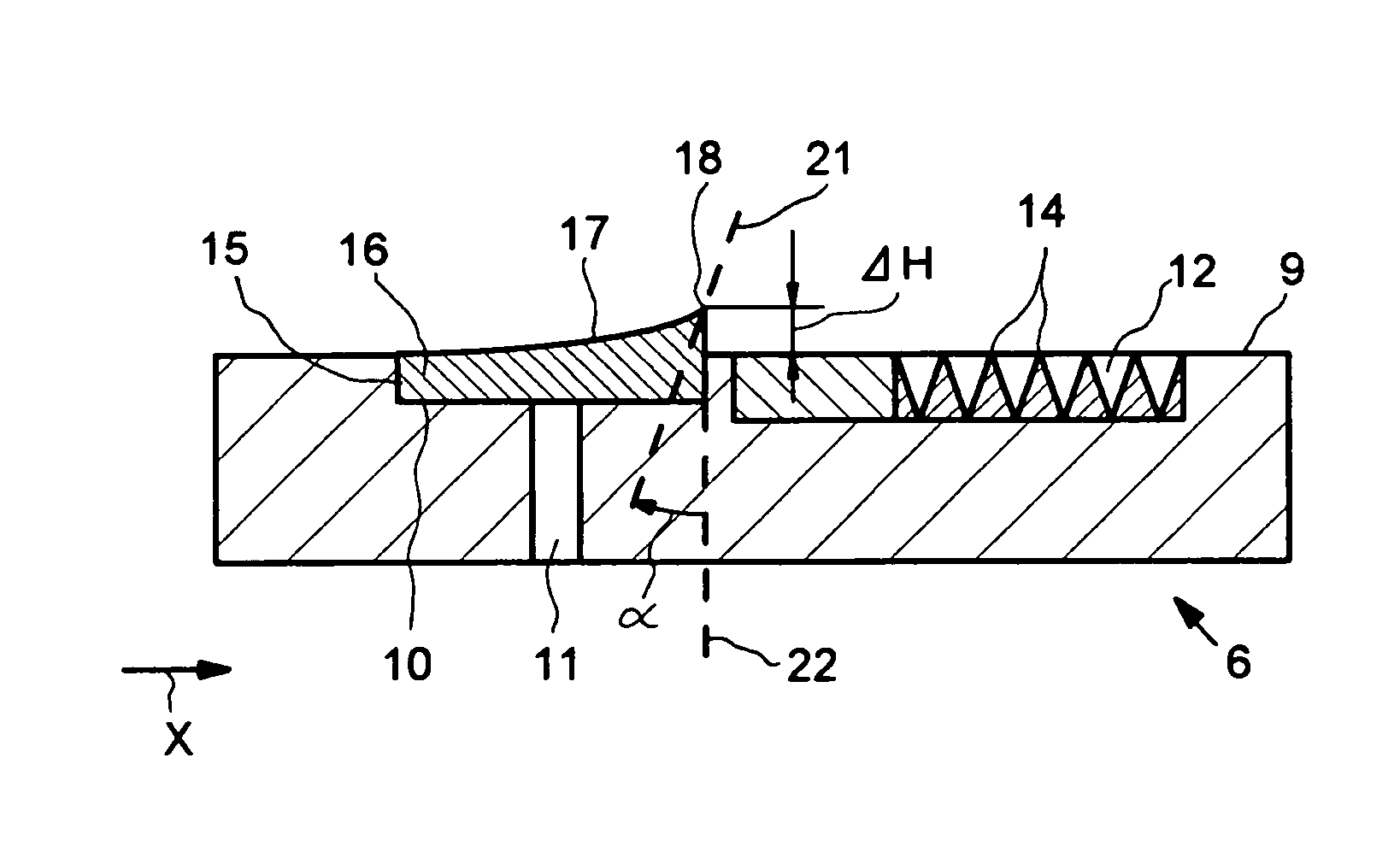
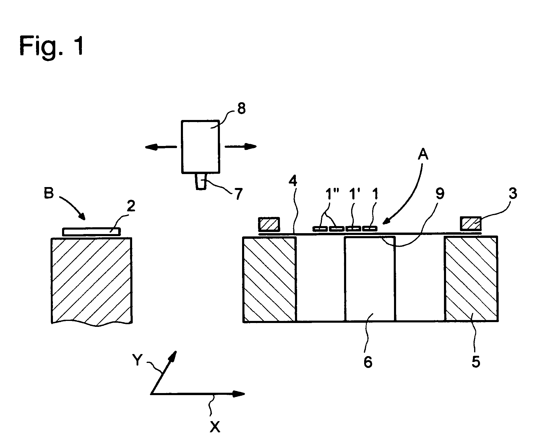
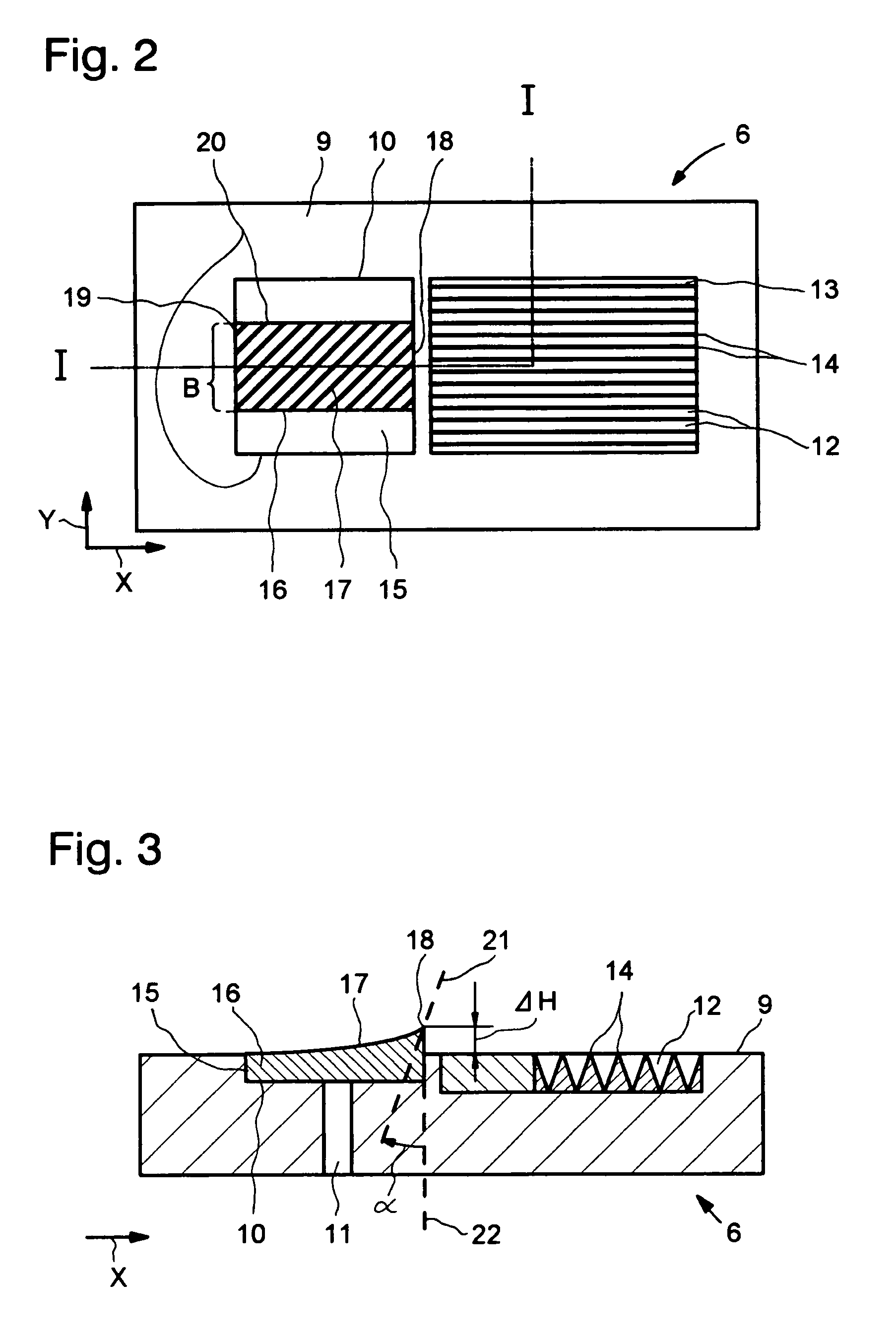
[0047]FIG. 1 shows a simplified, schematic representation of an apparatus for mounting semiconductor chips 1, 1′, 1″ onto a substrate 2. The semiconductor chips 1, 1′, 1″ arranged in rows and columns adhere to a foil 4 held for example in a frame 3. The apparatus has a movable wafer table 5, that accommodates the frame 3 and presents one semiconductor chip 1 after the other at a first location A. At the first location A, a chip ejector 6 in accordance with the invention, in this example one without needles, is arranged underneath the foil 4. On removal of the semiconductor chip 1, the chip ejector 6 serves to support its detachment from the foil 4. The wafer table 5 is movable in two orthogonal directions x and y. The foil 4 is arranged so that the edges of the semiconductor chips 1, 1′, 1″′ are almost parallel to the directions x and y. The apparatus also has a chip gripper 7 for transporting the semiconductor chip 1 presented at the first location A to a second location B located ...


PUM


Abstract

The detachment of a semiconductor chip (1) from a foil (4) and picking the semiconductor chip (1) from the foil (4) takes place with the support of a chip ejector (6), that has a ramp (16), the surface (17) of which is formed concave and ends at a stripping edge (18) projecting from the surface (9) of the chip ejector (6), and a support area (13) with grooves (12) arranged next to the stripping edge (18). Vacuum can be applied to the grooves (12). The detachment and picking of the semiconductor chip (1) from the foil (4) takes place in that the wafer table (5) is shifted relative to the chip ejector (6) in order to pull the foil (4) over the stripping edge (18) protruding from the surface (9) of the chip ejector (6), whereby the semiconductor chip (1) temporarily detaches itself at least partially from the foil (4) and lands on the foil (4) above the support area (13), and in that the chip gripper (7) picks the semiconductor chip (1) presented on the support area (13).

Description

PRIORITY CLAIM[0001]The present application claims priority under 35 U.S.C § 119 based upon European Patent Application No. 04101498.6 filed on Apr. 13, 2004, European Patent Application No. 04103054.5 filed on Jun. 29, 2004 and European Patent Application No. 04106169.8 filed on Nov. 29, 2004, the disclosures of which are hereby incorporated herein by reference as if set forth fully herein.FIELD OF THE INVENTION[0002]The invention concerns a method for detaching a semiconductor chip from a foil and an apparatus for mounting semiconductor chips that is suitable for carrying out the method.BACKGROUND OF THE INVENTION[0003]Typically, the semiconductor chips are presented on a foil held in a frame, also known in the trade as a tape, for processing with such a mounting apparatus. The semiconductor chips adhere to the foil. The frame with the foil is accommodated by a movable wafer table. The wafer table is shifted in cycles so that one semiconductor chip after the other is presented at ...

Claims


Application Information

Patent Timeline
Patent Type & Authority Patents(United States)
IPC IPC(8): H01L21/00H01L21/68H01L21/52
CPCH01L21/67132H01L21/68H01L2221/6839Y10T156/1132Y10T156/1121Y10T156/1922Y10T156/1944G07F11/1657G07F9/02F21V33/00F21Y2115/10
Inventor MEDDING, JONATHANLUSTENBERGER, MARTINANIEDERHAUSER, MARCELSCHNETZLER, DANIELSTALDER, ROLAND
Owner ESEC
Why Eureka
Try Eureka