Wafer level chip scale package

a chip scale and waver technology, applied in the field of miniature chip scale packages, can solve the problems of solder joint fatigue flip chip package damage, etc., and achieve the effect of high conformity

Inactive Publication Date: 2007-07-10
NAT SEMICON CORP
View PDF17 Cites 7 Cited by
  • Summary
  • Abstract
  • Description
  • Claims
  • Application Information

AI Technical Summary

Benefits of technology

[0017]To achieve the foregoing, and in accordance with the purpose of the present invention, the present invention includes wafer level chip scale integrated circuit package devices and methods for forming wafer level chip scale integrated circuit packages which provide highly compliant interconnections between external substrates and the packaged integrated circuit die and, additionally, provide flexibility in locating the external contacts which may be connected to other substrates.

Problems solved by technology

A disadvantage of this design is that stresses introduced on the contact bumps may damage the flip chip package.
As the solder joint in this design is a relatively rigid joint structure, the relative movement can deform and stress the contact bumps 106 and may ultimately result in damage to the flip chip package 100, for example, solder joint fatigue.
However, the addition of the underfill layer 112 results in an extra processing step and increased associated costs, thus impacting overall production costs and production yield.
Thus, this design tends to limit the packaging to use with smaller die sizes / pin counts, for example, 3×3 mm size / 28–40 leads.
This package, however, is not manufactured at the wafer level, and instead, the package is formed using individual chips singulated from a wafer.
Again, however, this package is not manufactured at the wafer level, and instead, the package is formed using individual chips singulated from a wafer.

Method used


Image

  • Wafer level chip scale package
  • Wafer level chip scale package
  • Wafer level chip scale package

Examples


Embodiment Construction

[0032]Methods and apparatus for a wafer level chip scale integrated circuit package are described below. In the following description, numerous specific details are set forth in order to provide a thorough understanding of the present invention. It will be appreciated, however, to one skilled in the art, that the present invention may be practiced without some or all of these specific details. In other instances, well known process operations have not been described in detail in order not to unnecessarily obscure the present invention.

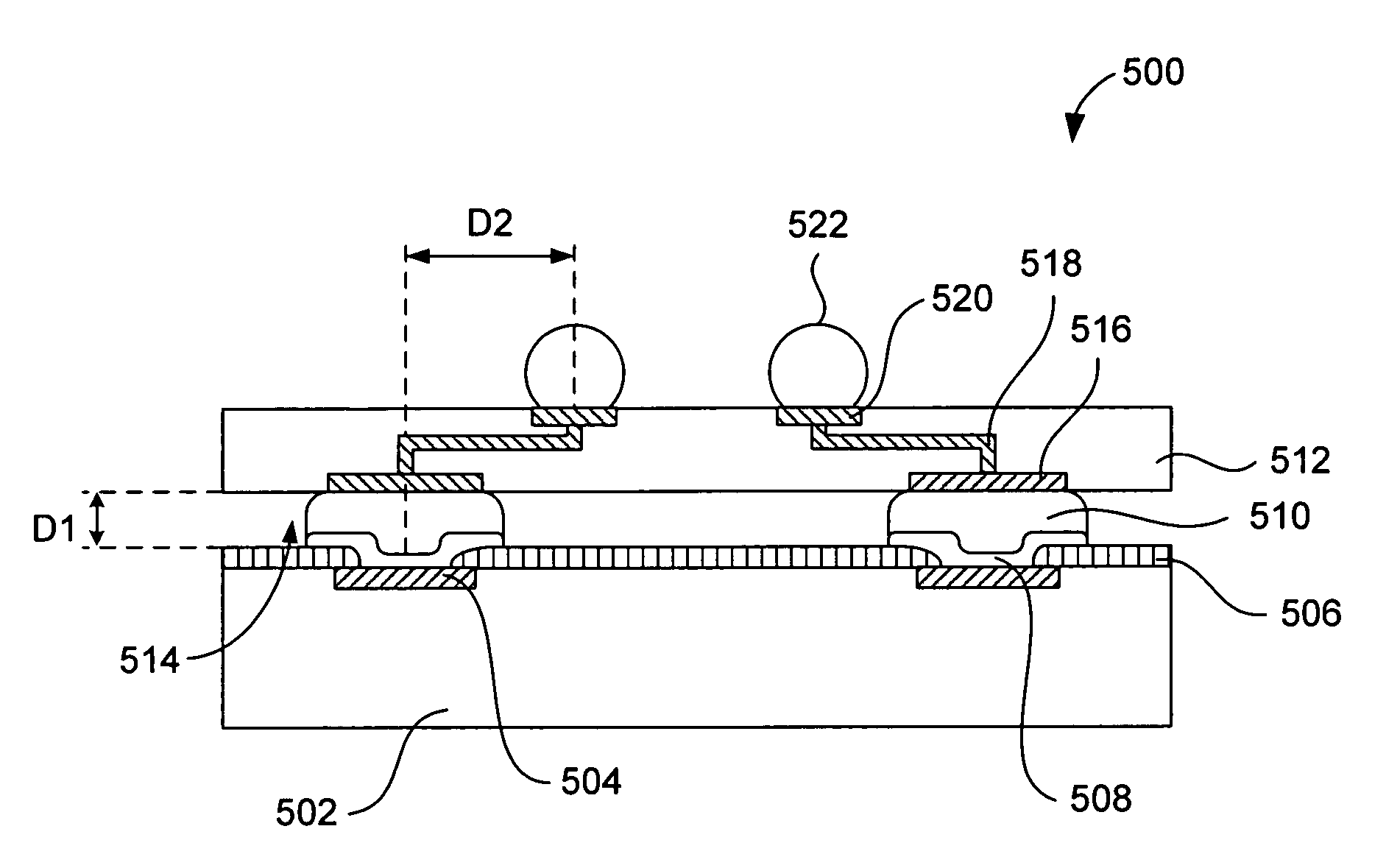
[0033]FIG. 4 is a diagrammatic side view illustration of a portion of a wafer level chip scale integrated circuit package 400 in accordance with one embodiment of the present invention. The package 400 includes an integrated circuit die 402 having a plurality of bond pads 404 formed on the top surface that provide external electrical contacts to various integrated circuit structures within the die. Typically, the top surface of the integrated circuit d...


PUM


Abstract

A wafer level fabricated integrated circuit package having an air gap formed between the integrated circuit die of the package and a flexible circuit film located over and conductively attached to the die though raised interconnects formed on the die is described. The flexible circuit film further includes routing conductors that connect inner landings on the bottom surface of the flexible circuit film with outer landings on the top surface of the flexible circuit film. The outer landings are offset a horizontal distance from the inner landings. In some embodiments, contact bumps are formed on the outer landings of the flexible circuit film layer for use in connecting the package to other substrates. The wafer level chip scale package provides a highly compliant connection between the die and any other substrate that the die is attached to.

Description

CROSS-REFERENCE TO RELATED APPLICATIONS[0001]This application is a Divisional of U.S. patent application Ser. No. 09 / 653,925, filed on Sep. 1, 2000 now U.S. Pat. No. 6,900,532, the contents of which is hereby incorporated by reference.FIELD OF THE INVENTION[0002]The present invention relates generally to integrated circuit packages. More specifically, the present invention relates to miniature chip scale packages manufactured in wafer form and improved package structures.BACKGROUND OF THE INVENTION[0003]With current emphasis on increased circuit density and decreased integrated circuit package footprints, process engineers attempt to design increasingly smaller and more dense integrated circuit packages. A current outgrowth of this emphasis is the chip scale package. Typically, a chip scale package has an overall package dimension that is relatively close to that of the integrated circuit die, or chip, that is enclosed within the package. Generally, chip scale packages are manufactu...

Claims


Application Information

Patent Timeline
Patent Type & Authority Patents(United States)
IPC IPC(8): H01L21/00H01L21/44H01L23/498
CPCH01L23/49827H01L23/4985H01L24/94H01L2224/16H01L2224/94H01L2924/01013H01L2924/15174H01L2924/15184H01L2924/15311H01L2224/81H01L2924/01033H01L2924/14H01L2224/05022H01L2224/05571H01L2224/05573H01L2224/05001H01L2224/05572H01L2224/05624H01L2924/00014H01L2224/16237H01L24/05H01L24/13H01L24/16H01L2924/181H01L2924/00H01L2224/05099H01L2924/00012
Inventor KELKAR, NIKHIL VISHWANATHTAKIAR, HEM P.
Owner NAT SEMICON CORP
Why Eureka
Try Eureka