SRAM cell for soft-error rate reduction and cell stability improvement

a technology of soft errors and cell stability, applied in semiconductor devices, digital storage, instruments, etc., can solve the problems of soft errors, small cmos devices, and significant challenges, and achieve the effect of cell stability improvement and soft error rate reduction

Active Publication Date: 2007-08-14
TAIWAN SEMICON MFG CO LTD
View PDF5 Cites 55 Cited by
  • Summary
  • Abstract
  • Description
  • Claims
  • Application Information

AI Technical Summary

Problems solved by technology

Significant challenges, however, are faced as the sizes of CMOS devices continue to decrease.
One such challenge is soft errors.
Soft errors are errors that occur in the logic state of a circuit due to excess charge carriers, which are typically induced by alpha-particles and cosmic ray neutrons.
Soft errors occurring in SRAM devices or other memory devices can cause the stored data to become corrupted.
These attempts, however, generally require additional circuitry, additional processing, and increased power requirements.
Such requirements may adversely affect the design and fabrication of more robust memory circuits.

Method used


Image

  • SRAM cell for soft-error rate reduction and cell stability improvement
  • SRAM cell for soft-error rate reduction and cell stability improvement
  • SRAM cell for soft-error rate reduction and cell stability improvement

Examples


third embodiment

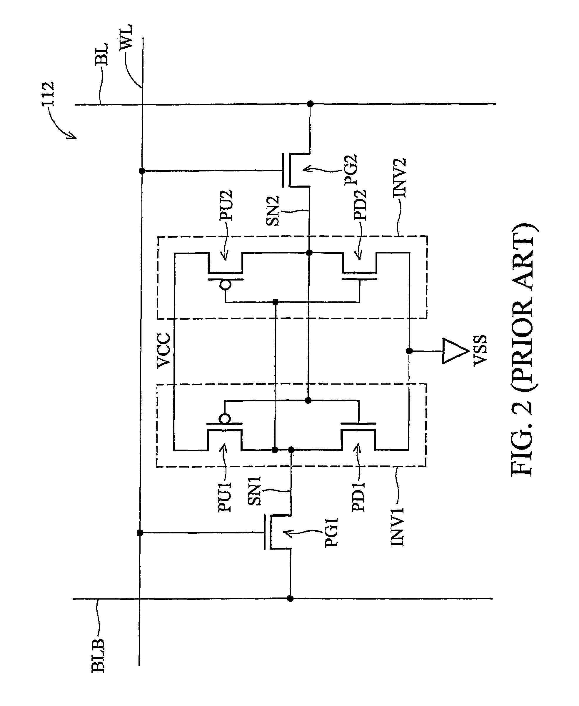
[0036]In accordance with a third illustrative embodiment of the present invention, also shown in FIG. 4, the channel width ratio of the pull up transistor channel width WPU1 to the pass gate transistor channel width PG1 is within a range of about 3 to about 1.2. The same range of ratios applies to the channel width ratio of the pull up transistor channel width WPU2 and the pass gate transistor channel width WPG2 in the

fourth embodiment

[0037]In accordance with a fourth illustrative embodiment of the present invention as shown in FIG. 4, the channel area ratio of the pull up transistor channel area APU1 to the pass gate transistor channel area APG1 is within a range of about 3.5 to about 1.25. The same range of ratios applies to the channel area ratio of the pull up transistor channel area APU2 to the pass gate transistor channel area APG2 in the

[0038]It is recognized that the first, second, third, and fourth illustrative embodiments may be combined in any suitable manner that optimizes memory cell performance. For example, a channel area ratio of about 1.75 may be applied between the channel areas APU1 to APG1, as well as the channel areas APU2 to APG2. In the same memory cell, a channel width ratio of about 1.25 may exist between the channel widths WPU1 to WPD1, and the channel widths WPU2 to WPD2.

fifth embodiment

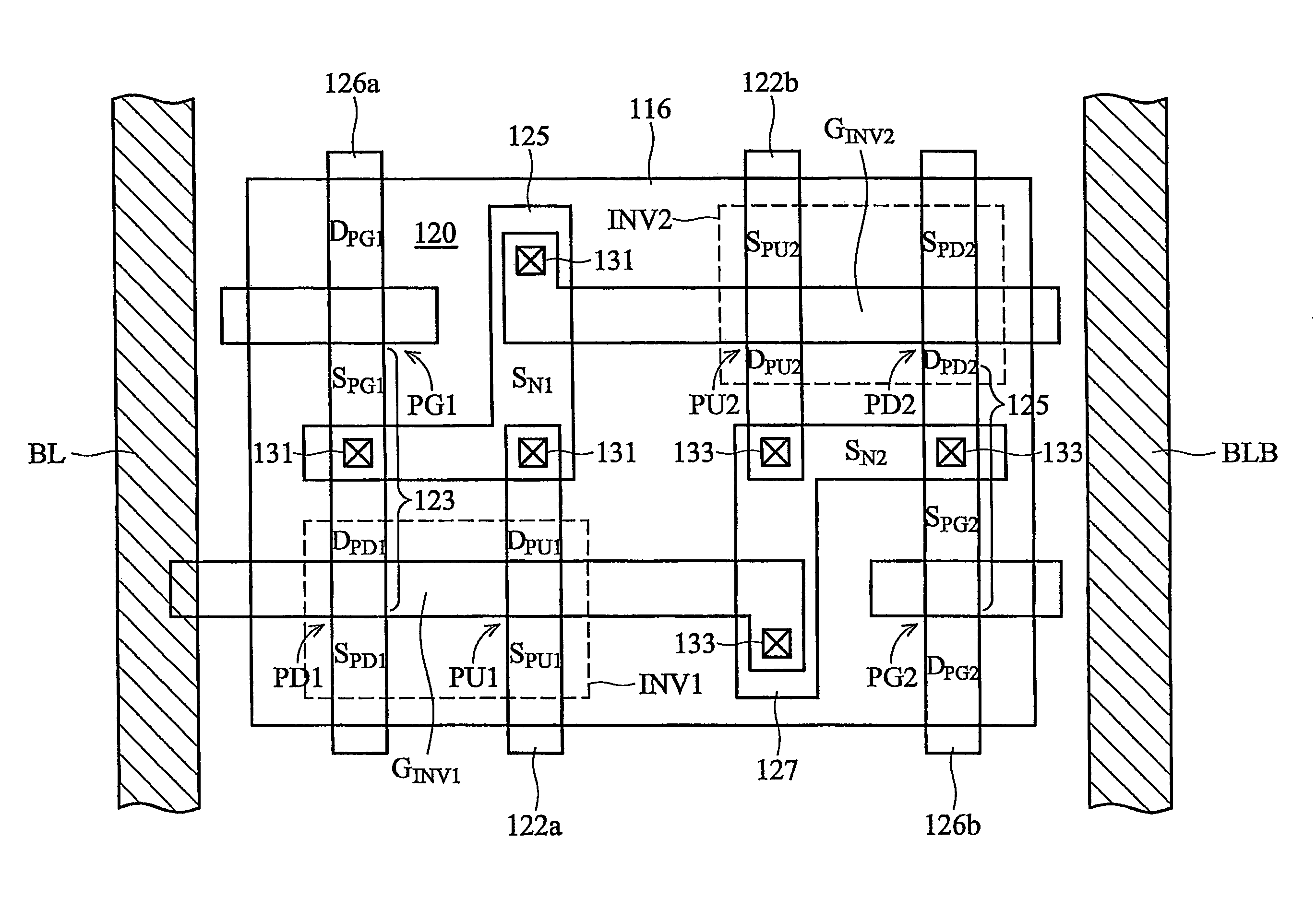
[0039]With reference to FIG. 7, a fifth illustrative embodiment includes an SRAM memory cell 112 similar to those shown in FIGS. 2 through 4. However, as shown in FIG. 5, the memory cell 112 of the fifth embodiment has a capacitor C1 electrically connected to the storage node SN1 and a capacitor C2 electrically connected to the storage node SN2. Illustrative embodiments preferably include SRAM memory cells having one capacitor electrically connected to each storage node.

[0040]A cross section along the line 6-6 in FIG. 6 is shown in FIG. 8. With combined reference to FIGS. 6, 7 and 8, the fifth illustrative embodiment will be further described. The first electrode E1 of the capacitor C1 is the metal wire 128 at the node SN1. The metal wire 128 is preferably a copper wire on the first layer of metal M1 overlying the substrate surface 140. The metal wire 128 may alternatively be a buried interconnect or a butted contact, for example. Placing a copper wire 142 on a second metal layer M2...


PUM


Abstract

An SRAM device includes a memory cell. The memory cell includes a first cross-coupled inverter and a second cross-coupled inverter, which is electrically connected to the first cross-coupled inverter. Each inverter includes a pull down device and a pull up device. The pull up device is electrically connected to the pull down device. A channel width ratio of the pull up device to the pull down device is preferably within a range of about 1.5 to about 0.8. A channel area ratio of the pull up device to the pull down device is preferably within a range of about 3 to about 1. A pass gate device is electrically connected to the pull down device. A channel width ratio of the pull up device to the pass gate device is preferably within a range of about 3.0 to about 1.2.

Description

[0001]This application claims priority to Provisional Application Ser. No. 60 / 575,217, filed on May 28, 2004, and entitled “SRAM Cell for Soft-Error Rate Reduction and Cell Stability Improvement”, which application is hereby incorporated herein by reference.TECHNICAL FIELD[0002]The present invention relates generally to a system and method for providing semiconductor devices, and more particularly to a system and method for providing a static random access memory (SRAM) cell for soft-error rate reduction and cell stability improvement.BACKGROUND[0003]Complementary metal-oxide-semiconductor (CMOS) technology is the dominant semiconductor technology used for the manufacture of ultra-large scale integrated (ULSI) circuits today. Size reduction of the semiconductor structures has provided significant improvement in the speed, performance, circuit density, and cost per unit function of semiconductor chips over the past few decades. Significant challenges, however, are faced as the sizes ...

Claims


Application Information

Patent Timeline
Patent Type & Authority Patents(United States)
IPC IPC(8): G11C11/00G11C11/412H01L21/8244H01L27/11
CPCG11C11/4125H01L27/11H01L27/1104H10B10/00H10B10/12
Inventor LIAW, JHON-JHY
Owner TAIWAN SEMICON MFG CO LTD
Why Eureka
Try Eureka