The problem with this type of probing assembly is that the needle-like tips, due to their narrow geometry, exhibit high inductance so that signal distortion is large in high frequency measurements made through these tips.
Also, these tips can act in the manner of a planing tool as they wipe across their respective pads, thereby leading to excessive pad damage.
This problem is magnified to the extent that the probe tips bend out of shape during use or otherwise fail to terminate in a common plane which causes the more forward ones of the tips to bear down too heavily on their respective pads.
Also, it is impractical to mount these tips at less than 100 micron center-to-center spacing or in a multi-row grid-like pattern so as to accommodate the pad arrangement of more modern, higher density dies.
Also, this type of probing assembly has a scrub length of the needle tips of 25 microns or more, which increases the difficulty of staying within the allowed probing area.
However, although several different forms of this probing assembly have been proposed, difficulties have been encountered in connection with this type of assembly in reducing pad wear and in achieving reliable clearing of the oxide layer from each of the device pads so as to ensure adequate electrical connection between the assembly and the device-under-test.
In respect to both of these devices, however, because of manufacturing tolerances, certain of the contact bumps are likely to be in a recessed position relative to their neighbors and these recessed bumps will not have a satisfactory opportunity to engage their pads since they will be drawn away from their pads by the action of their neighbors on the rigid support.
Furthermore, even when “scrub” movement is provided in the manner of Huff, the contacts will tend to frictionally cling to the device as they perform the scrubbing movement, that is, there will be a tendency for the pads of the device to move in unison with the contacts so as to negate the effect of the contact movement.
Hence this form of membrane probing assembly does not ensure reliable electrical connection between each contact and pad.
These alternative devices, however, do not afford sufficient pressure between the probing contacts and the device pads to reliably penetrate the oxides that form on the pad surfaces.
Pad damage is likely to occur with this type of design, however, because a certain amount of tilt is typically present between the contacts and the device, and those contacts angled closest to the device will ordinarily develop much higher contact pressures than those which are angled away.
The same problem arises with the related assembly shown in European Patent Pub.
However, the Evans device is subject to the friction clinging problem already described insofar as the pads of the device are likely to cling to the contacts as the support pivots and causes the contacts to shift laterally.
In both Crumly and Barsotti, however, if any tilt is present between the contacts and the device at the time of engagement, this tilt will cause the contacts angled closest to the device to scrub further than those angled further away.
A further disadvantage of the Crumly device, in particular, is that the contacts nearer to the center of the membrane will scrub less than those nearer to the periphery so that scrub effectiveness will vary with contact position.
It is difficult, however, to originally position these fingers so that they all terminate in a common plane, particularly if a high density pattern is required.
Moreover, these fingers are easily bent out of position during use and cannot easily be rebent back to their original position.
Nor, in Evans at least, is there an adequate mechanism for tolerating a minor degree of tilt between the fingers and pads.
Although Evans suggests roughening the surface of each finger to improve the quality of electrical connection, this roughening can cause undue abrasion and damage to the pad surfaces.
Yet a further disadvantage of the contact fingers shown in both Evans and Higgins is that such fingers are subject to fatigue and failure after a relatively low number of “touchdowns” or duty cycles due to repeated bending and stressing.
Unfortunately, the aforementioned construction technique results in a structure with many undesirable characteristics.
The excess pressure may also result in bending and breaking of the probe station, the probe head, and / or the membrane probing assembly.
In addition, the devices with the greatest height may damage the pads on the test device because of the increased pressure required to make suitable contact for the devices with the lowest height.
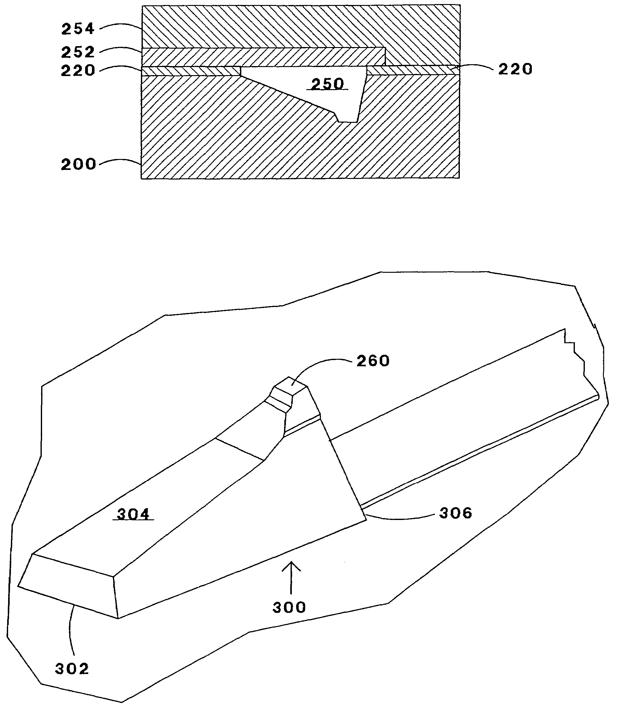
Second, the ability to decrease the pitch (spacing) between the devices is limited by the “mushrooming” effect of the electroplating process over the edges of the polyimide 77 and photoresist layers 79 and 81.
The “mushrooming” effect is difficult to control and results in a variable width of the beams 90, contact bumps 92, and contacting portions 93.
Third, it is difficult to plate a second metal layer directly on top of a first metal layer, such as contacting portions 93 on the contact bumps 92, especially when using nickel.
Unfortunately, the interface seed layer reduces the lateral strength of the device due to the lower sheer strength of the interface layer.
Fourth, applying a photoresist layer over a non-uniform surface tends to be semi-conformal in nature resulting in a non-uniform thicknesses of the photoresist material itself.
With variable photoresist thickness it is difficult to properly process the photoresist to provide uniform openings.
Fifth, separate alignment processes are necessary to align the beams 90 on the traces 76a, the contact bumps 92 on the beams 90, and the contacting portions 93 on the contact bumps 92. Each alignment process has inherent variations that must be accounted for in sizing each part. The minimum size of the contacting portions 93 is defined primarily by the lateral strength requirements and the maximum allowable current density therein. The minimum size of the contacting portions 93, accounting for the tolerances in alignment, in turn defines the minimum size of the contact bumps 92 so that the contacting portions 93 are definitely constructed on the contact bumps 92. The minimum size of the contact bumps 92, in view of the contacting portions 93 and accounting for the tolerances in alignment, defines the minimum size of the beams 90 so that the contact bumps 92 are definitely constructed on the beams 90. Accordingly, the summation of the tolerances of the contact bumps 92 and the contacting portions 93, together with a minimum size of the contacting portions 93, defines the minimum device size, and thus defines the minimum pitch between contact pads.

