Stacked connector assembly
a connector and assembly technology, applied in the field of stacked connector assemblies, can solve the problems of limited difficulty in conserving component area on the circuit board,
- Summary
- Abstract
- Description
- Claims
- Application Information
AI Technical Summary
Benefits of technology
Problems solved by technology
Method used
Image

Examples
Embodiment Construction
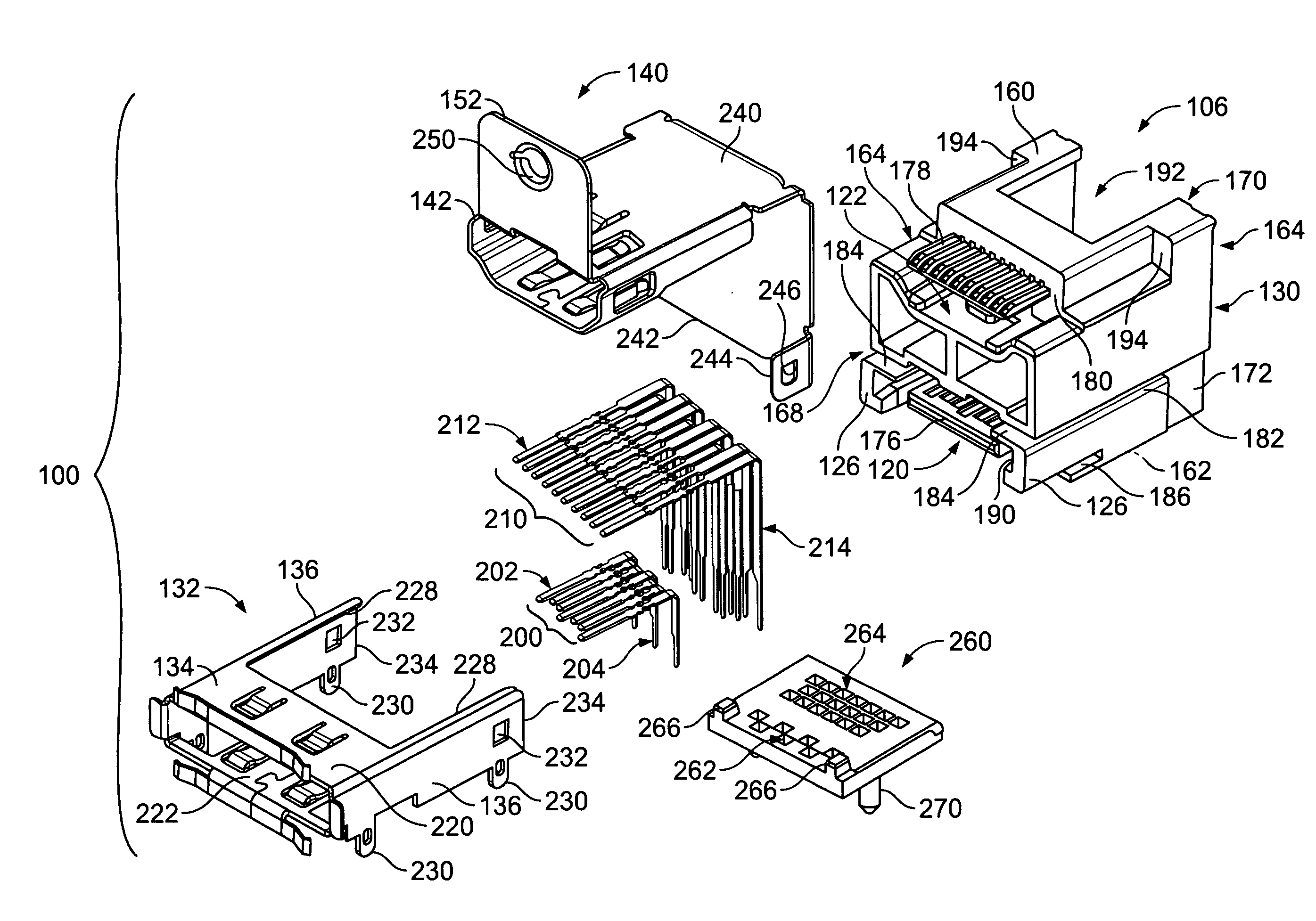
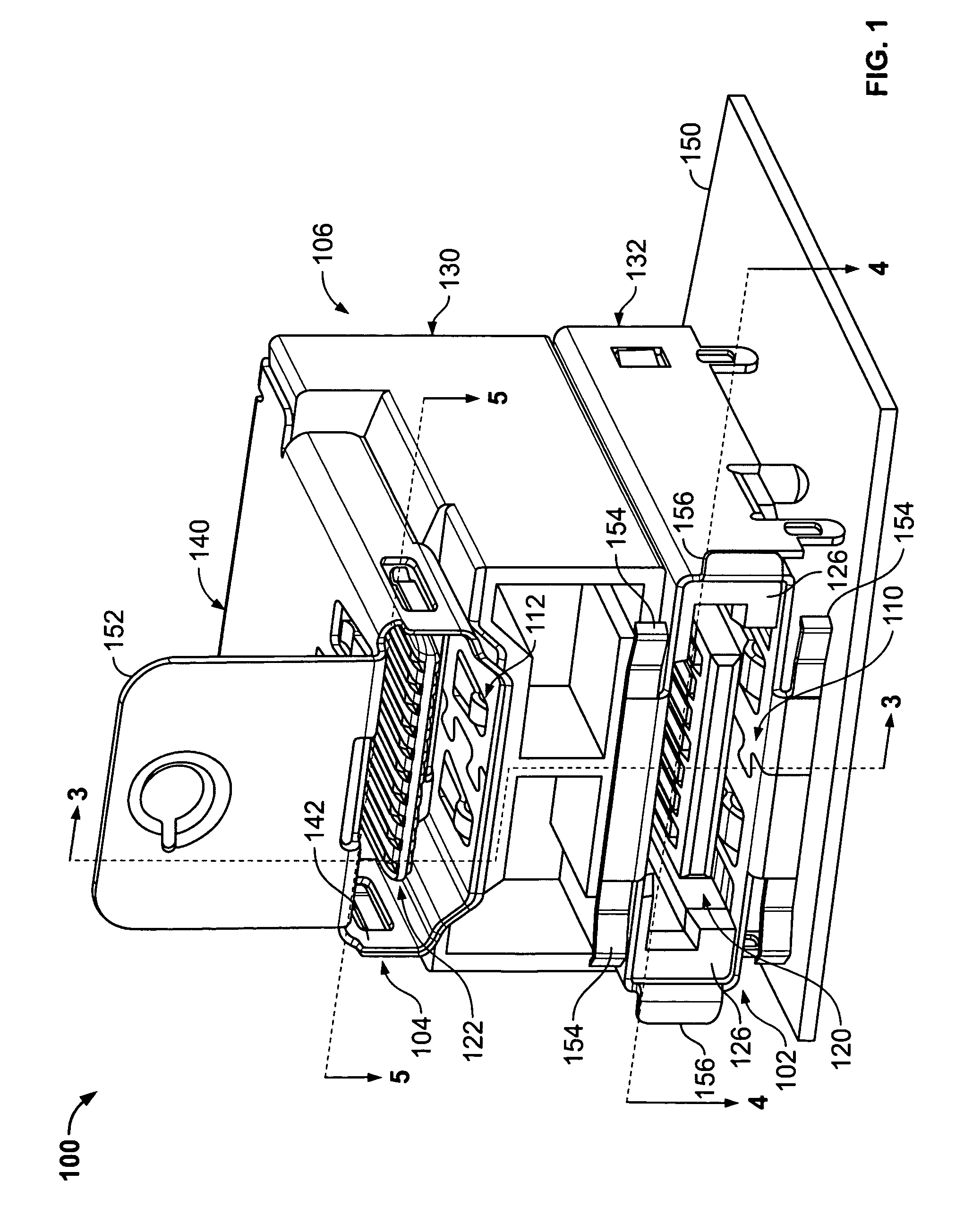
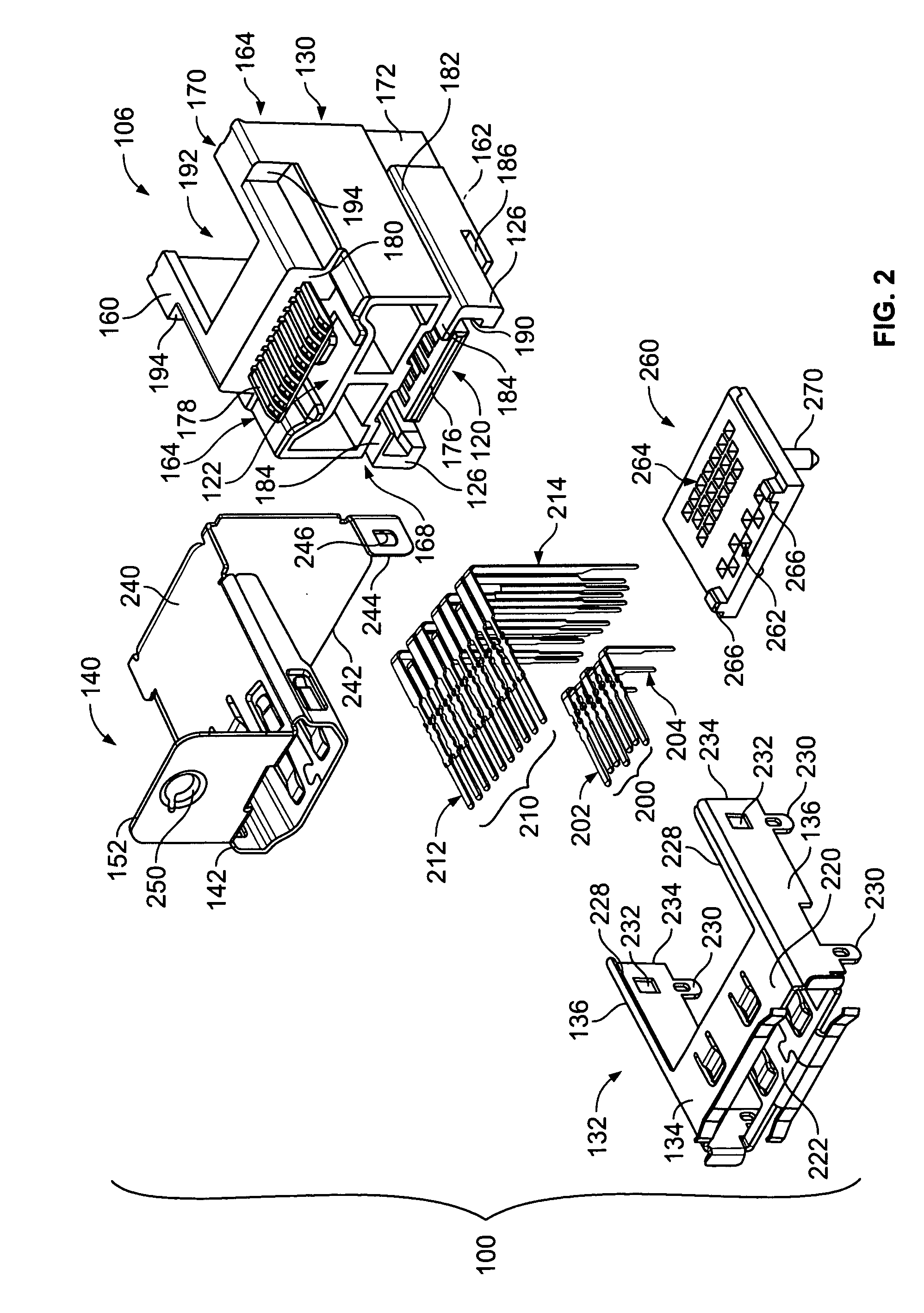
[0018]FIG. 1 illustrates a stacked connector assembly 100 formed according to an exemplary embodiment of the present invention. The connector assembly 100 includes a first or lower connector 102 and a second or upper connector 104. The upper connector 104 is stacked above the lower connector 102. The connectors 102 and 104 have a common housing 106 and mating faces 110 and 112, respectively, that are substantially coplanar. The housing 106 includes a lower contact area 120 and a second or upper contact area 122. A lower shield 132 includes a shroud 134 (FIG. 2) that surrounds the lower contact area 120. An upper shield 140 includes a shroud 142 that surrounds the upper contact area 122. The lower contact area 120 and shroud 134 define the lower connector 102 and the upper contact area 122 and upper shroud 142 define the upper connector 104. In an exemplary embodiment, the lower connector 102 may comprise an eSATA connector and the upper connector 104 may comprise an HDMI connector. ...
PUM
 Abstract
Description
Claims
Application Information
 - Generate Ideas
- Intellectual Property
- Life Sciences
- Materials
- Tech Scout
- Unparalleled Data Quality
- Higher Quality Content
- 60% Fewer Hallucinations
Browse by: Latest US Patents, China's latest patents, Technical Efficacy Thesaurus, Application Domain, Technology Topic, Popular Technical Reports.
© 2025 PatSnap. All rights reserved.Legal|Privacy policy|Modern Slavery Act Transparency Statement|Sitemap|About US| Contact US: help@patsnap.com