Image sensors for reducing dark current and methods of fabricating the same

a technology of image sensor and dark current, applied in the field of image sensor, can solve the problems of image defects such as pixel saturation, deterioration of charge transmission efficiency and charge storage capacity, and inconvenient use of cmos image sensor

Active Publication Date: 2007-09-18
SAMSUNG ELECTRONICS CO LTD
View PDF15 Cites 27 Cited by
  • Summary
  • Abstract
  • Description
  • Claims
  • Application Information

AI Technical Summary

Problems solved by technology

One major difference between CMOS image sensors and a CCD image sensors, however, is the manner in which the electrical charges corresponding to each photodiode are transformed into electrical voltages.
A number of problems may occur in conventional CMOS image sensors due to the presence of dark current or other forms of noise.
For example, dark current is known to deteriorate charge transmission efficiency and charge storage capacity, which can lead to image defects such as pixel saturation.
However, these methods are limited to reducing dark current only within specific portions of a unit pixel.
Such defects result from fabrication processes performed on the semiconductor substrate, silicon dangling bonds, or the like.
The output voltage resulting from the defects is added to the output voltage caused by incident light, thereby causing image defects such as white spots on images.

Method used


Image

  • Image sensors for reducing dark current and methods of fabricating the same
  • Image sensors for reducing dark current and methods of fabricating the same
  • Image sensors for reducing dark current and methods of fabricating the same

Examples


Embodiment Construction

[0025]Exemplary embodiments of the invention are described below with reference to the corresponding drawings. These embodiments are presented as teaching examples. The actual scope of the invention is defined by the claims that follow.

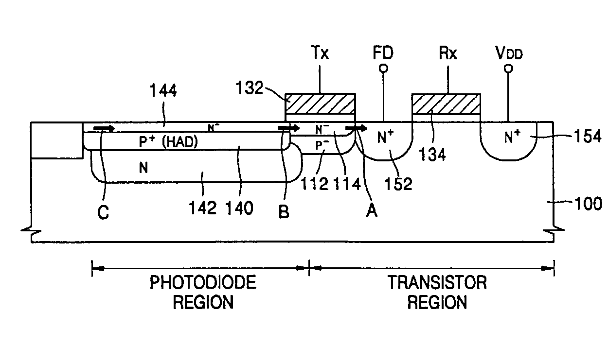
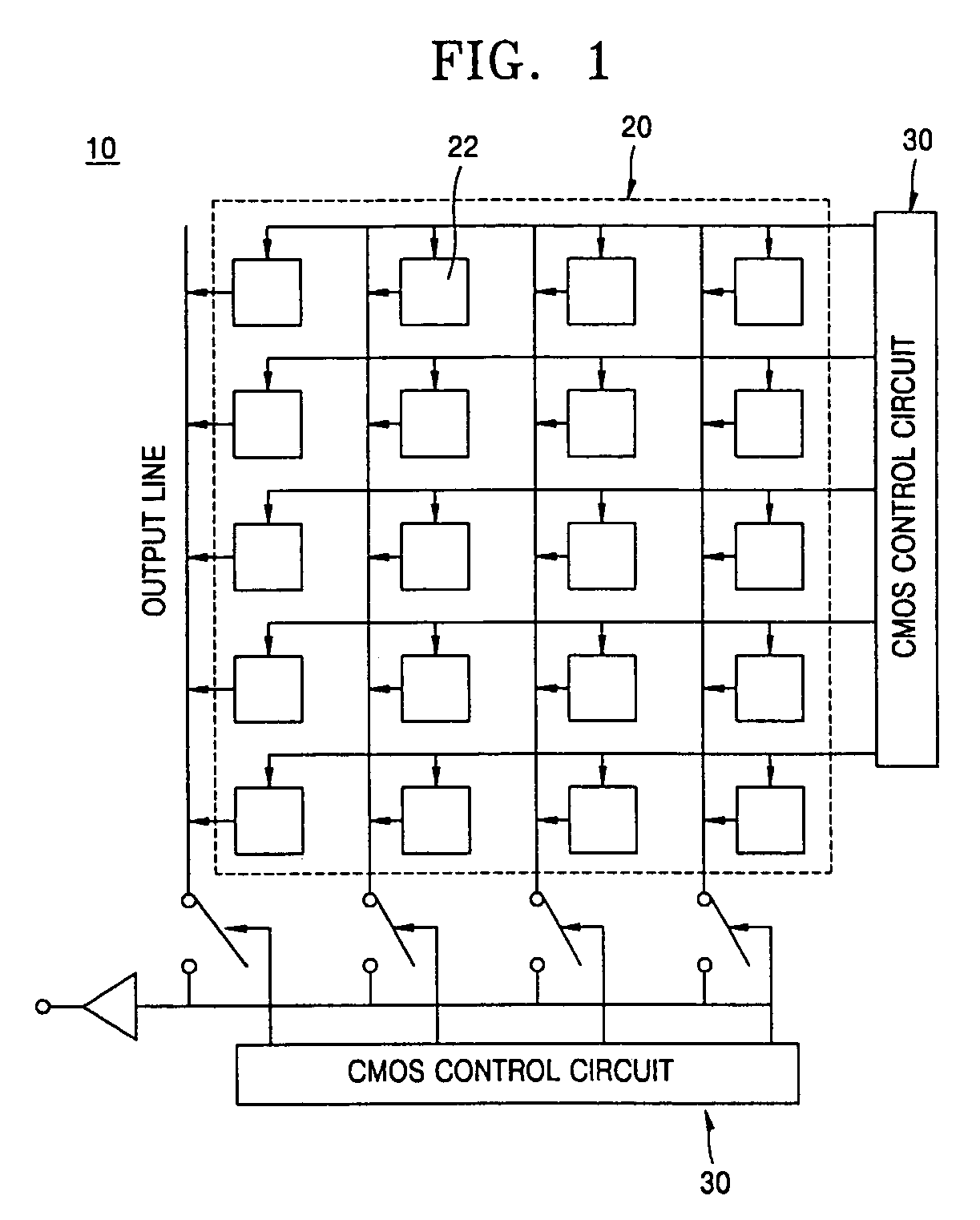
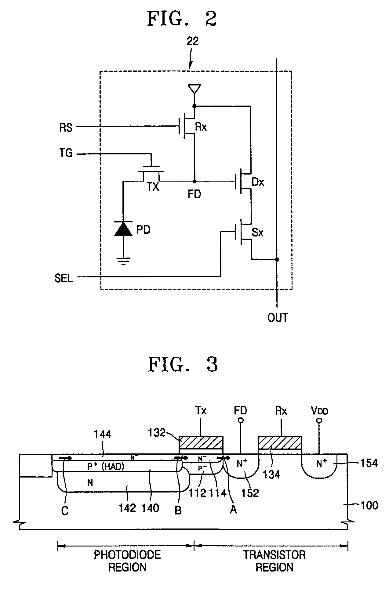
[0026]FIG. 1 illustrates an example in which an embodiment of the present invention is configured as a CMOS image sensor (CIS) 10. CIS 10 generally includes an active pixel array 20 and CMOS control circuitry 30. As is schematically shown in FIG. 1, pixel array 20 includes a plurality of active pixels 22 generally arranged in matrix form. Word lines are respectively connected to pixels 22 of each row of pixel array 20, and bit lines are respectively connected to pixels 22 of each column of pixel array 20. CMOS control circuitry 30 includes a row decoder for selecting rows (word lines) of pixel array 20, and a column decoder for selecting columns (bit lines) of pixel array 20. Selected bit lines are connected to an output amplifier via switching elemen...


PUM


Abstract

An image sensor includes a semiconductor substrate of a first conductivity type, a photodiode of a second conductivity type located in the substrate, a hole accumulated device (HAD) region of the first conductivity type located over the photodiode, a thin surface diffusion region formed on the surface of the HAD region, and a transfer gate located over the surface of the substrate adjacent the HAD region. The image sensor further includes a first channel region of the first conductivity type located in the substrate and aligned below the transfer gate, a second channel region of the second conductivity type located in the substrate between said transfer gate and the first channel region, and an floating diffusion region which is located in the substrate and which electrically contacts the second channel region.

Description

CROSS-REFERENCE TO RELATED APPLICATIONS[0001]This is a continuation-in-part of, and a claim of priority is made to, non-provisional U.S. patent application Ser. No. 11 / 032,147, filed Jan. 11, 2005 now U.S. Pat. No. 7,214,974, the contents of which are incorporated herein by reference in its entirety.[0002]A claim of priority is also made to Korean Patent Applications Nos. 2004-40900, 2004-89255, and 2004-90444, filed respectively on Jun. 4, 2004, Nov. 4, 2004, and Nov. 8, 2004, the contents of which are incorporated herein by reference in their entirety.BACKGROUND OF THE INVENTION[0003]1. Field of the Invention[0004]The present invention relates generally to an image sensor used to transform optical signals into electrical signals. More particularly, the invention relates to a complementary metal oxide semiconductor (CMOS) image sensor and a method of fabricating the same.[0005]2. Description of the Related Art[0006]Complementary metal-oxide semiconductor (CMOS) image sensors (CISs)...

Claims


Application Information

Patent Timeline
Patent Type & Authority Patents(United States)
IPC IPC(8): H01L27/148H01L21/00H01L27/146H01L31/0352H01L31/062
CPCH01L27/14603H01L27/14609H01L27/14683H01L27/14689H01L31/035281
Inventor PARK, CHANSHIN, JONG-CHEOL
Owner SAMSUNG ELECTRONICS CO LTD
Why Eureka
Try Eureka