Solid-state imaging apparatus, driving method of the same and imaging system

a driving method and imaging system technology, applied in the direction of television system, radioation control device, instruments, etc., can solve the problems of cross talk or color mixture or photo response non-uniformity (prnu), increased dark current, and increased probability of escaping generated electric charg

Active Publication Date: 2010-07-01
CANON KK
View PDF11 Cites 73 Cited by
  • Summary
  • Abstract
  • Description
  • Claims
  • Application Information

AI Technical Summary

Problems solved by technology

In this case, there arises a problem in that dark current increases due to depletion of a substrate surface constituting an MOS transistor of the transfer element.
However, if photoelectric conversion is performed for a long time in a state where the electric charge is accumulated in the photodiode, the internal electric field of the photodiode continues to be weak during the photoelectric conversion period, thereby increasing the probability

Method used


Image

  • Solid-state imaging apparatus, driving method of the same and imaging system
  • Solid-state imaging apparatus, driving method of the same and imaging system
  • Solid-state imaging apparatus, driving method of the same and imaging system

Examples


first embodiment

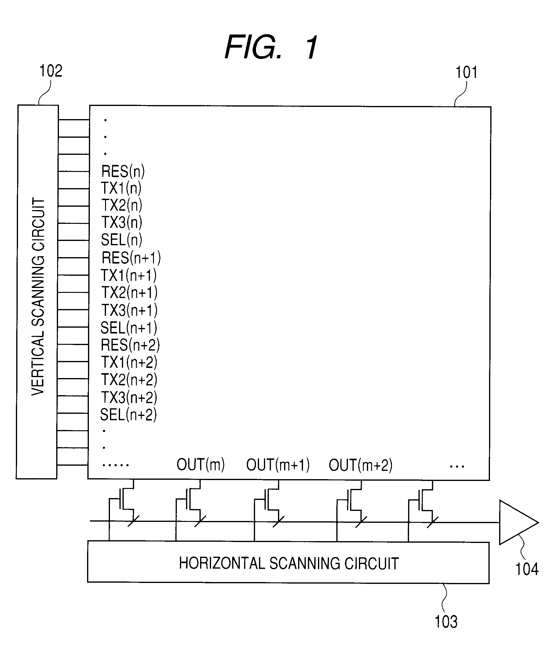
[0027]FIG. 1 is a schematic block diagram illustrating a configuration example of a solid-state imaging apparatus according to a first embodiment of the present invention. FIG. 2 is an equivalent circuit diagram of a pixel contained in an imaging area 101. FIG. 3 is a sectional view illustrating a case where a pixel illustrated in FIG. 2 is formed on a semiconductor substrate. FIG. 4 is a timing chart illustrating a driving method of driving the solid-state imaging apparatus.

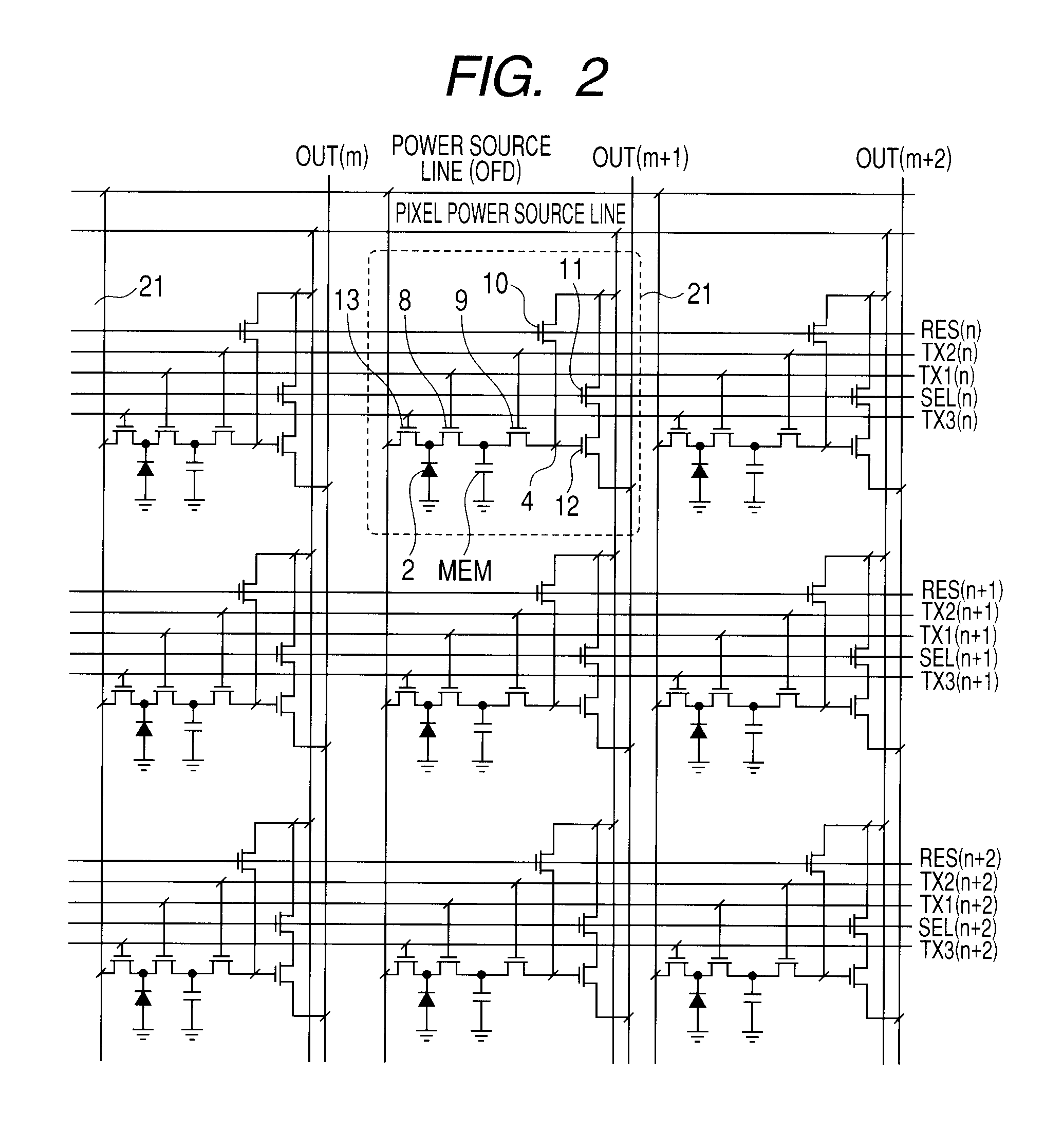
[0028]In FIG. 1, the solid-state imaging apparatus includes an imaging area 101 in which a plurality of pixels is provided, a vertical scanning circuit 102 which is a control element and a horizontal scanning circuit 103. Here, the pixels provided in the imaging area 101 are assumed to be arranged in a matrix shape. The horizontal scanning circuit 103 sequentially scans signal lines each corresponding to a pixel column of the imaging area 101 and causes an output circuit 104 to output a signal for each of a row ...

second embodiment

[0067]Hereinafter, the driving method of driving the solid-state imaging apparatus according to a second embodiment of the present invention will be described in detail by referring to the accompanying drawings. The second embodiment is the same as the first embodiment except that the first transfer element 8 is a surface channel transistor. FIG. 6 is a sectional view illustrating a case where a pixel according to the present embodiment is formed on a semiconductor substrate. FIG. 6 corresponds to FIG. 3 of the first embodiment. In FIG. 6, a P-type semiconductor region 601 may have the same impurity concentration as that of the P-type semiconductor region 201 or may have a different impurity concentration from that of the P-type semiconductor region 201.

[0068]FIGS. 8A to 8F illustrate a potential state of a pixel at an individual timing from immediately before time t0 to the end of accumulation time, of the timings illustrated in FIG. 4. The second embodiment of FIGS. 8A to 8F are d...

third embodiment

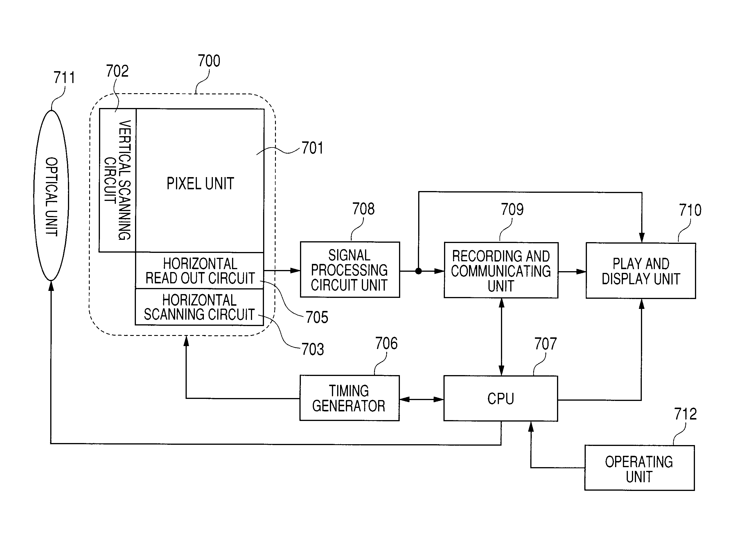
[0072]FIG. 7 illustrates a configuration example of the solid-state imaging system according to a third embodiment of the present invention. The imaging system is an imaging system to which the solid-state imaging apparatus of the first embodiment or second embodiment is applied. For example, the imaging system includes an optical unit 711, a solid-state imaging apparatus 700, a signal processing circuit unit 708, a recording and communicating unit 709, a timing generator 706, a CPU 707, a play and display unit 710 and an operating unit 712.

[0073]The optical unit 711 which is an optical system such as a lens uses the pixel unit 701 which is located on the solid-state imaging apparatus 700 and has a plurality of pixels arranged in a two-dimensional shape so as to focus light from an object on the pixel unit 701 to form an object image. The pixel unit 701 includes the aforementioned imaging area 101. At a timing based on a signal from the timing generator 706, the solid-state imaging ...


PUM


Abstract

A solid-state imaging apparatus has a plurality of pixels, wherein each of the pixels includes: a photoelectric conversion element for converting incident light to an electric charge; an accumulating element accumulating the electric charge converted by the photoelectric conversion element; a first transfer element for transferring the electric charge converted by the photoelectric conversion element to the accumulating element; a second transfer element for transferring the electric charge accumulated in the accumulating element to a floating diffusion region; and an amplifying element for amplifying the electric charge in the floating diffusion region, wherein the first transfer element transfers the electric charge converted by the photoelectric conversion element to the accumulating element a plurality of times and causes the accumulating element to cumulatively accumulate the electric charge transferred the plurality of times.

Description

BACKGROUND OF THE INVENTION[0001]1. Field of the Invention[0002]The present invention relates to a solid-state imaging apparatus, a driving method of the same and an imaging system for use in a scanner, a video camera, a digital still camera and the like.[0003]2. Related Background Art[0004]In a conventional solid-state imaging apparatus, there has been generally known a pixel configured such that a photoelectric conversion element performing photoelectric conversion on incident light also serves as an accumulating element for accumulating an electric charge.[0005]In contrast to this, Japanese Patent Application Laid-Open No. 2004-111590 (hereinafter referred to simply as Patent Document 1) discloses a technique for providing the accumulating element separately from the photoelectric conversion element. According to Patent Document 1, a global shutter can be implemented by transferring the electric charge accumulated in the photoelectric conversion element from the photoelectric con...

Claims


Application Information

Patent Timeline
IPC IPC(8): H04N5/335H04N5/232H01L27/146H04N5/361H04N5/369H04N5/3745
CPCH04N5/3597H04N5/361H04N5/3741H04N5/335H04N25/626H04N25/63H04N25/766H04N25/00
Inventor SUGIYAMA, SHUICHIROYAMASHITA, YUICHIRO
Owner CANON KK
Why Eureka
Try Eureka