Amplification with feedback capacitance for photodetector signals

a photodetector and feedback capacitance technology, applied in the field of imager circuits, can solve the problems of limited output voltage swing and linearity of source follower amplifiers, limited output voltage swing on the downward side of the output voltage swing,

Active Publication Date: 2005-10-06
APTINA IMAGING CORP
View PDF4 Cites 74 Cited by
  • Summary
  • Abstract
  • Description
  • Claims
  • Application Information

AI Technical Summary

Benefits of technology

[0015] The present invention provides methods and apparatus in which photodetector signals are amplified with feedback capacitance. In exemplary embodiments, a difference signal is obtained from reset and signal outputs from a CTIA. A CTIA is operated at a low po

Problems solved by technology

Source follower amplifiers have a number of limitations when used in an APS.
Source follower amplifiers also have limited output swing and linearity.
In addition, the output voltage swing is limited on the downward side when the photodiode loses its reverse bias.
The dynamic range of an APS imager with source follower amplifiers is usually limited by the source follower.
These readout circuits, however, are designed for infrared detectors, which are characterized by sizeable backg

Method used


Image

  • Amplification with feedback capacitance for photodetector signals
  • Amplification with feedback capacitance for photodetector signals
  • Amplification with feedback capacitance for photodetector signals

Examples


Embodiment Construction

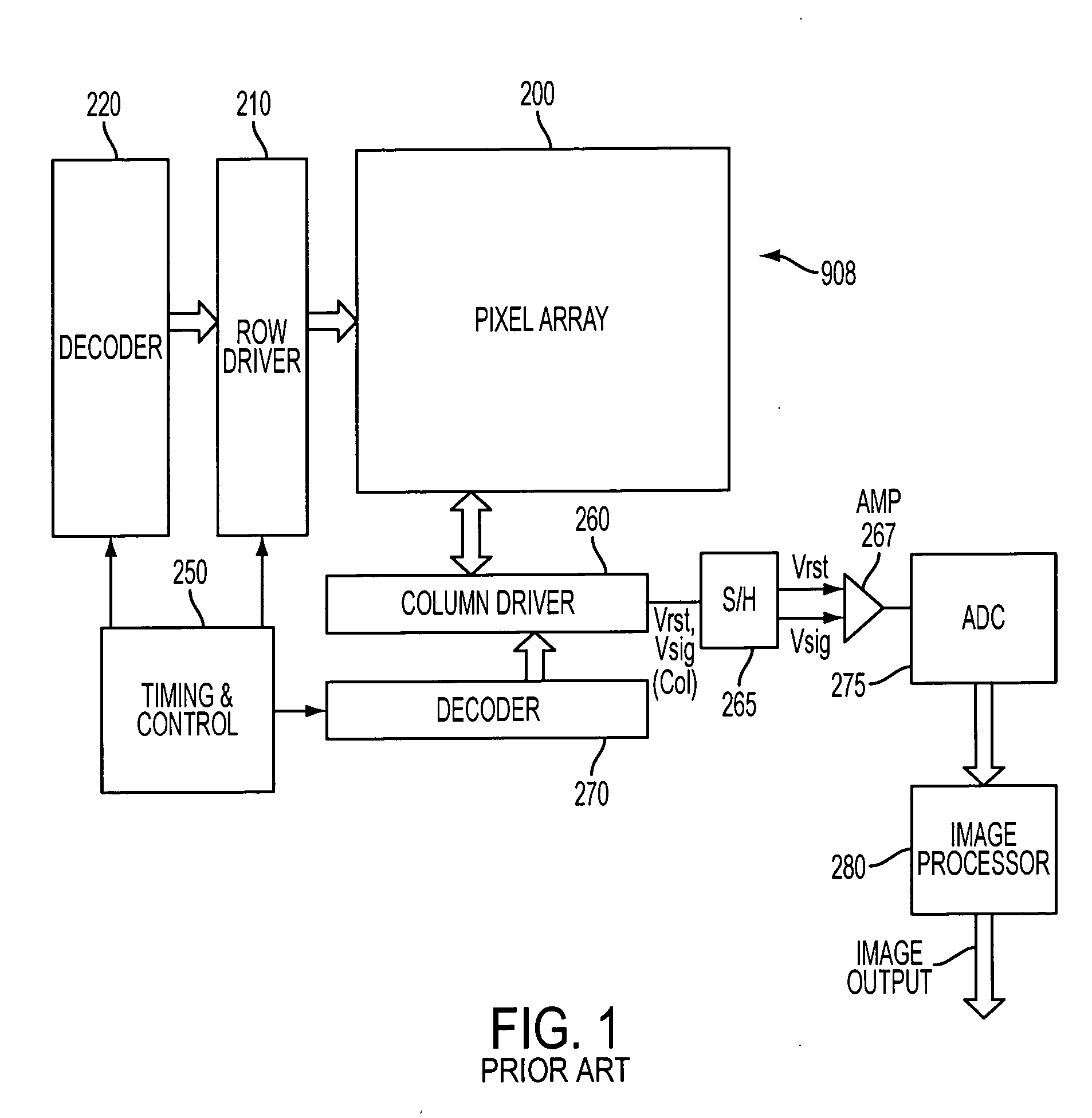
[0031] The present invention provides techniques that may be used in commercial applications of image sensors. Exemplary applications include monolithic visible image sensors and a variety of hybrid infrared focal plane arrays and stacked structure visible sensors.

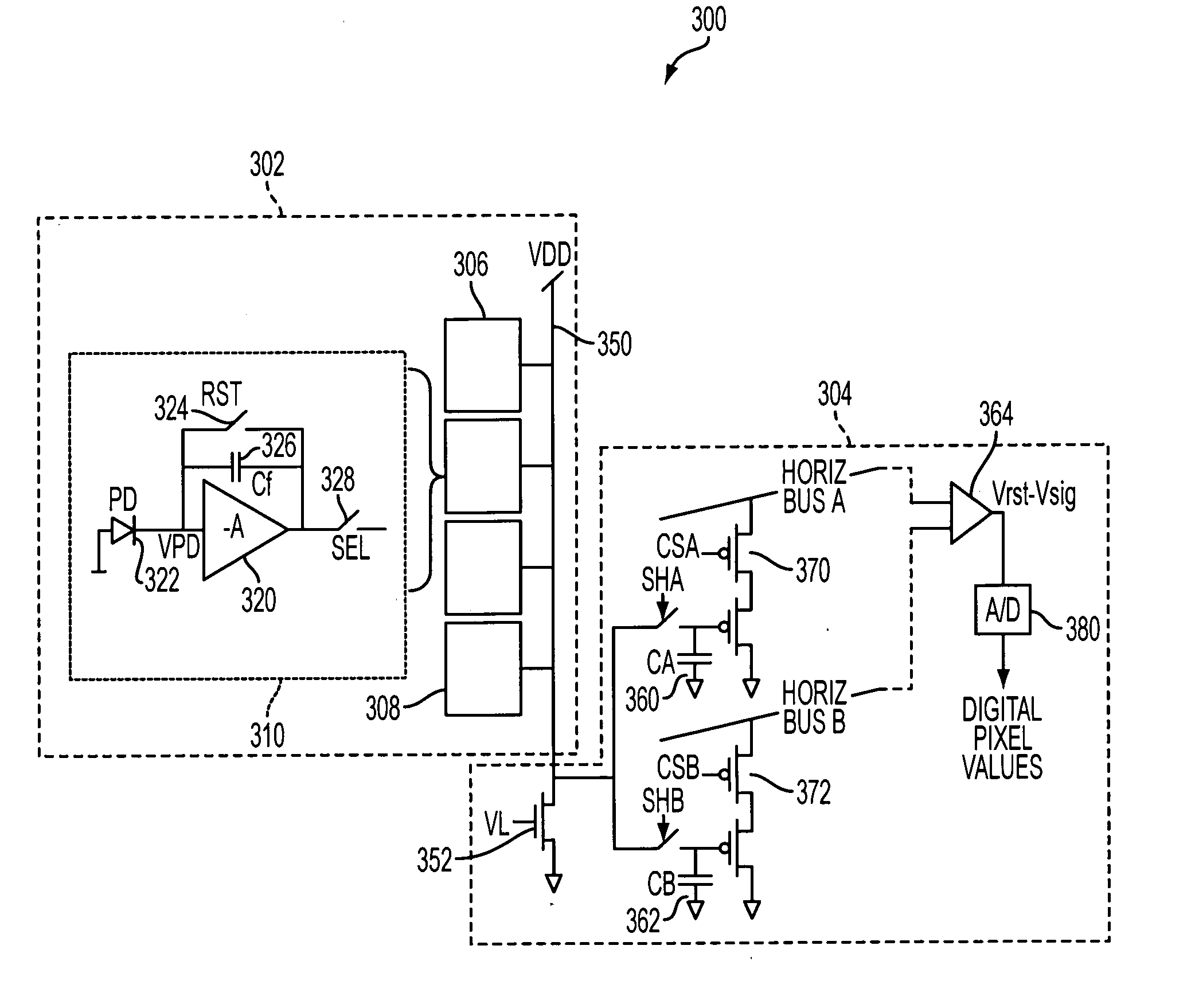
[0032] As used herein, the term “capacitive transimpedance amplifier” or “CTIA” includes any amplifying circuitry in which there is a capacitive feedback path unless otherwise specified. In a simple example, a capacitive element could be connected between the signal input and signal output leads of amplifying circuitry, but various other configurations can be implemented, such as with a primary capacitive element and an additional capacitor element that can be connected in parallel to increase capacitance.

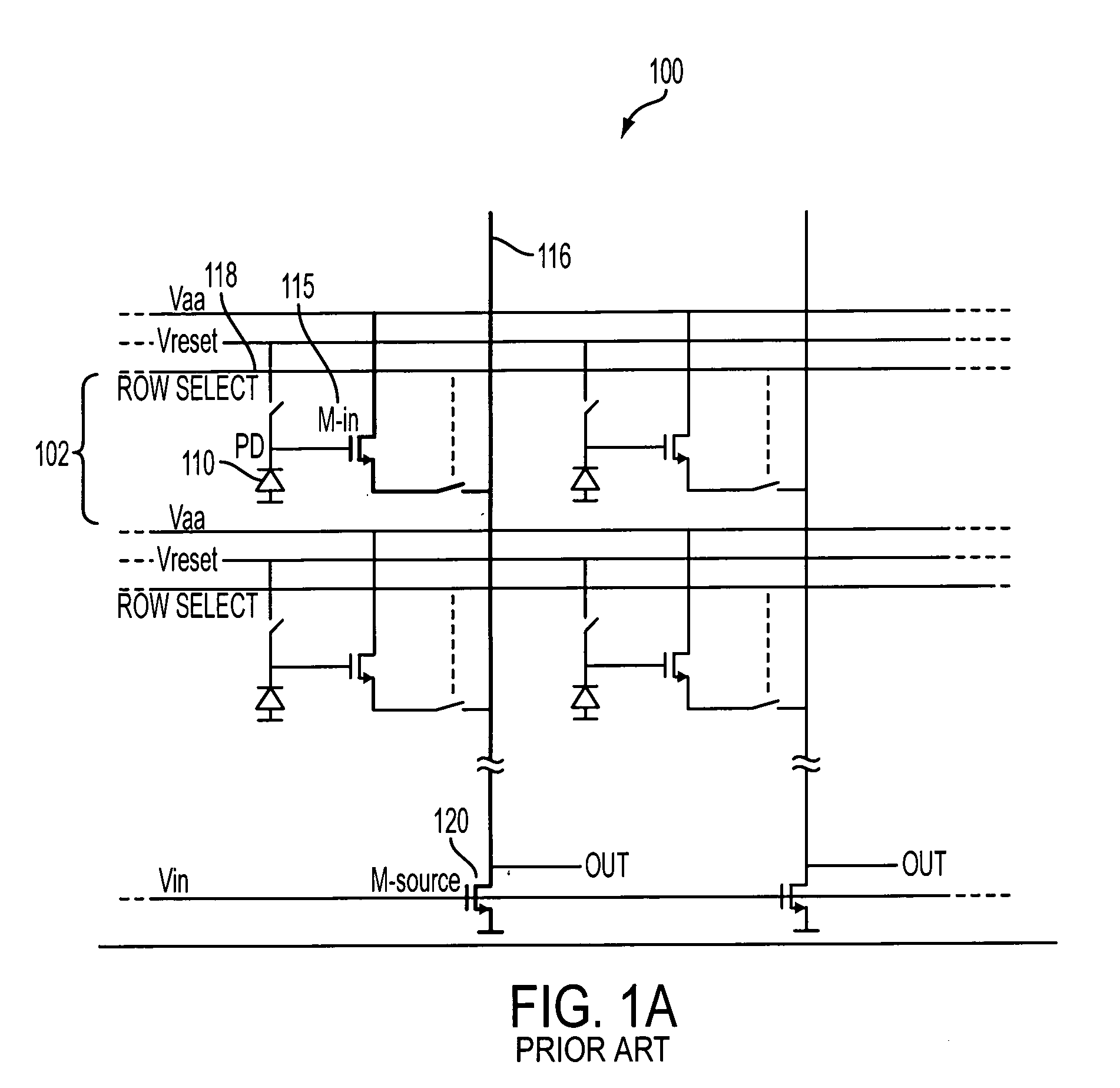
[0033] The pixels discussed herein are illustrated and described as inventive modifications to three transistor (3T) pixel circuits for the sake of example only. It should be understood that the invention may be used wi...


PUM


Abstract

Signals from an imager pixel photodetector are received by an amplifier having capacitive feedback, such as a capacitive transimpedance amplifier (CTIA). The amplifier can be operated at a low or no power level during an integration period of a photodetector to reduce power dissipation. The amplifier can be distributed, with an amplifier element within each pixel of an array and with amplifier output circuitry outside the pixel array. The amplifier can be a single ended cascode amplifier, a folded cascode amplifier, a differential input telescopic cascode amplifier, or other configuration. The amplifier can be used in pixel configurations where the amplifier is directly connected to the photodetector, or in configurations which use a transfer transistor to couple signal charges to a floating diffusion node with the amplifier being coupled to the floating diffusion node.

Description

FIELD OF THE INVENTION [0001] The present invention relates generally to imager circuits and, more specifically to circuits and methods for amplification of an output signal for pixel sensors. BACKGROUND OF THE INVENTION [0002] Various imager circuits have been proposed including charge coupled device (CCD) arrays, complementary metal oxide semiconductor (CMOS) arrays, arrays combining both CCD and CMOS features, as well as hybrid infrared focal-plane arrays (IR-FPAs). Conventional arrays have light-sensing elements, typically referred to as “pixels” and readout circuitry that provides signals indicating light sensed by the pixels. [0003] For example, a CMOS imager includes a focal plane array of pixel cells; each cell includes a photodetector, for example, a photogate, photoconductor or a photodiode overlying a substrate for producing a photo-generated charge in a doped region of the substrate. A readout circuit is provided for each pixel cell and includes at least a source followe...

Claims


Application Information

Patent Timeline
IPC IPC(8): H01L27/00H04N5/363H04N5/3745H04N5/378
CPCH03F3/08H04N3/1512H03F3/087H03F3/082H04N25/616H04N25/77H04N25/76H04N25/75
Inventor OLSEN, ALFFOSSUM, ERIC R.ROSSI, GIUSEPPE
Owner APTINA IMAGING CORP
Why Eureka
Try Eureka