High-low sensitivity pixel

a sensitivity pixel and high-low technology, applied in the field of high-low sensitivity pixel, can solve the problems of large variation in the represented signal, fixed pattern noise in the output image, active pixel sensor, etc., and achieve the effect of improving pixel density and reducing chip area

Active Publication Date: 2005-05-05
APTINA IMAGING CORP
View PDF2 Cites 73 Cited by
  • Summary
  • Abstract
  • Description
  • Claims
  • Application Information

AI Technical Summary

Benefits of technology

[0011] Under an alternate embodiment, several high-low sensitivity (HLS) pixels circuits are coupled together using a common output diode (i.e., floating diffusion node). Along with the output diode, the coupled HLS pixels also share a reset, source-follower, and select transistor, thus improving pixel density with a reduced chip area.

Problems solved by technology

However, most CMOS active pixel sensors have only 10 bits of output and 8 bits of resolution that are typically delivered to the user in most image formats such as JPEG.
First, the “knee point” in a linear-to-log transition is difficult to control, leading to fixed pattern noise in the output image.
Second, under low light, the log portion of the circuit is slow to respond, leading to lag.
Third, a logarithmic representation of the signal in the voltage domain (or charge domain) means that small variations in signal due to fixed pattern noise will lead to large variations in the represented signal.
This approach has architectural problems if the pixel is read out at different points in time since data must be stored in an on-board memory before the signals can be fused together.
However, the low gain portion of the pixel often presents color separation processing problems.
Furthermore, the idea of including capacitors in the pixel area has not been effectively developed, due to the limited area available on the pixel.
Since the pixel area is primarily used for light detection and readout circuitry, capacitors have not been effectively implemented in the pixel structure.

Method used


Image

  • High-low sensitivity pixel
  • High-low sensitivity pixel
  • High-low sensitivity pixel

Examples


Embodiment Construction

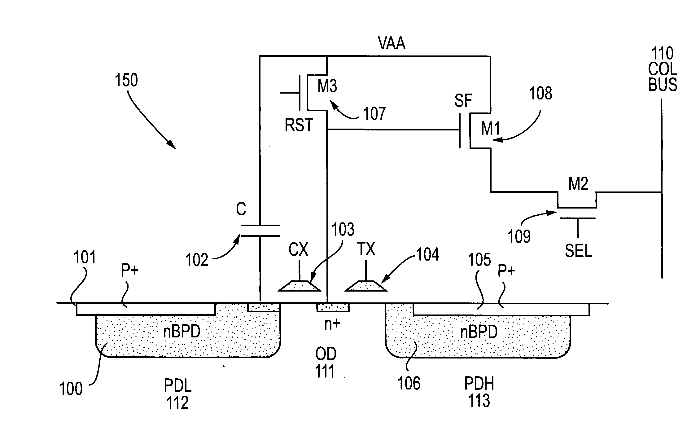
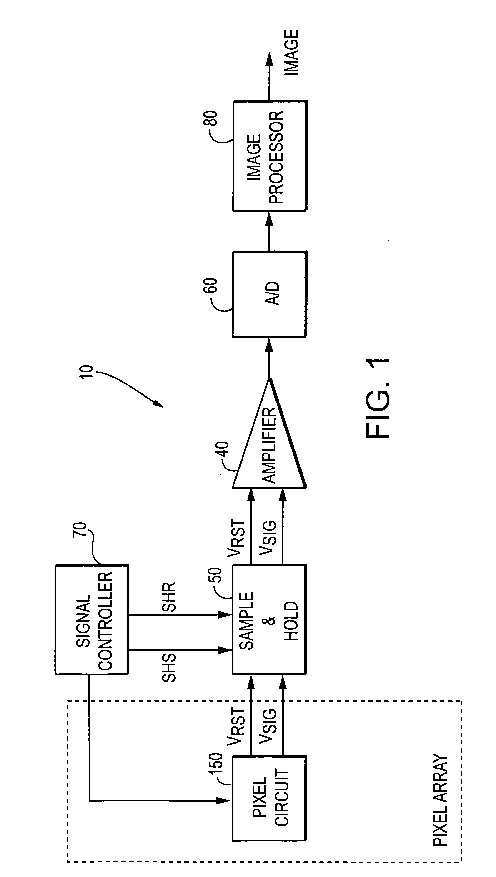
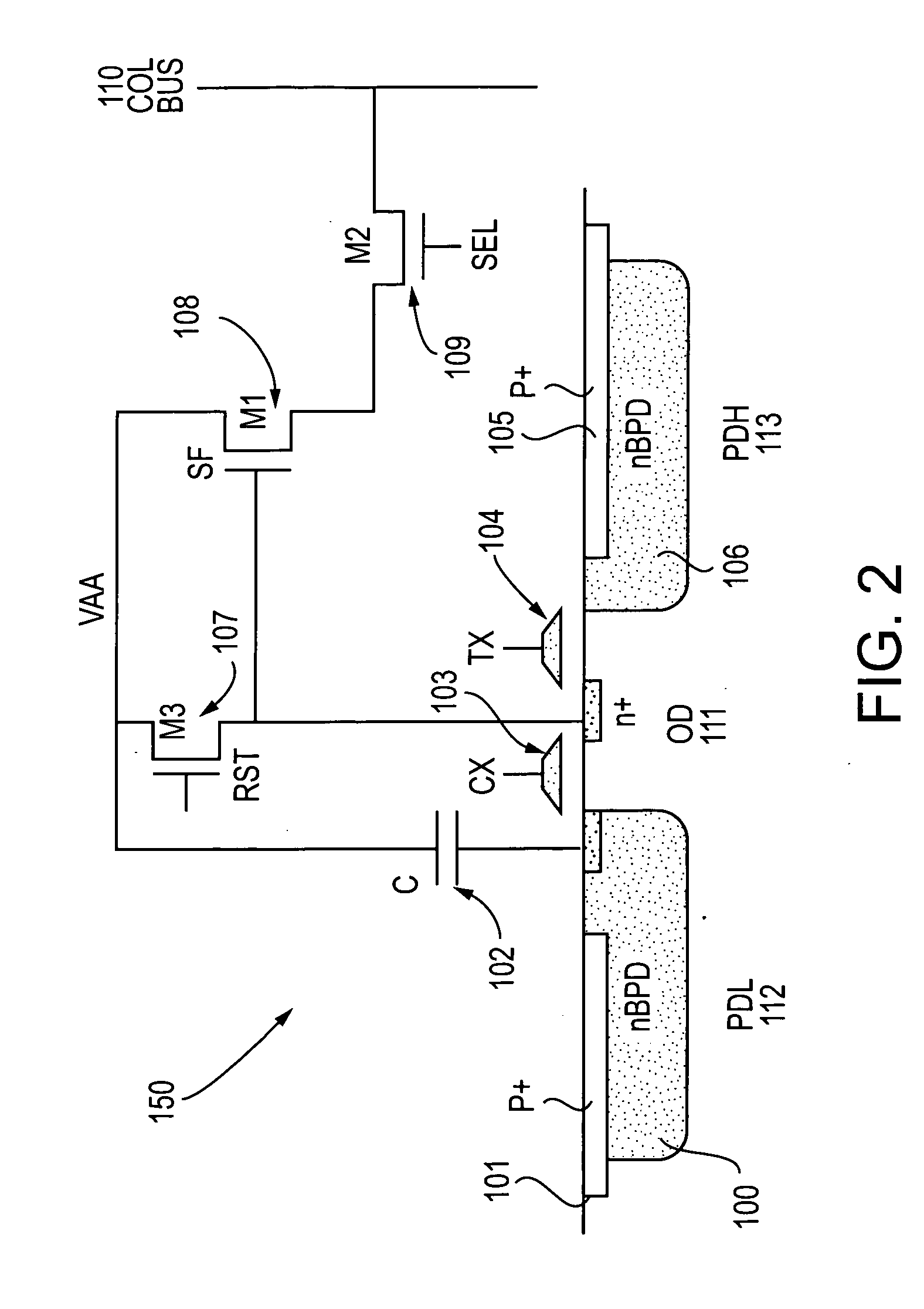
[0020] The present invention is used in a CMOS imaging device generally illustrated in FIG. 1 by reference numeral 10. The imaging device 10 includes an array of pixels arranged in rows and columns (not shown) with each pixel having a pixel circuit 150; each pixel in the array is associated with a column line to which all pixels of a same column are connected, the pixels being selected row-by-row. The pixel circuit 150 provides a reset signal VRST and a pixel image signal VSIG as outputs during reset and integration periods, respectively. The reset signal VRST and pixel image signal VSIG are then captured by a sample and hold circuit 50 associated with that column in response to sampling signals SHS (for the image signal) and SHR (for the reset signal), respectively. The sample and hold circuit 50 passes the sampled reset signal VRST and sampled image signal VSIG to an amplifier 40 which in turn provides a signal representing the difference between the reset signal and pixel image s...


PUM


Abstract

A pixel circuit, and a method for operating a high-low sensitivity (HLS) pixel circuit, to provide increased dynamic range in an imager. The pixel circuit combines a four transistor (“4T”) and a three-transistor plus capacitor (“3TC”) configuration in one pixel, where the 4T portion of the pixel is coupled to a high sensitivity buried photodiode region, and the 3TC portion of the pixel is coupled to a low sensitivity buried photodiode region. The pixel circuit first reads out charge from the high sensitivity photodiode region and compares it to a reset voltage, then reads out charge from the low sensitivity photodiode region. Under an alternate embodiment, multiple HLS pixels are coupled through a common floating diffusion node.

Description

[0001] The present invention relates to a pixel circuit and related method of operating a pixel circuit to increase intrascene dynamic range while reducing fixed pattern noise. BACKGROUND OF THE INVENTION [0002] Intrascene dynamic range refers to the range of incident light that can be accommodated by an image sensor in a single frame of pixel data. Examples of scenes that generate high dynamic range incident signals include an indoor room with outdoor window, an outdoor scene with mixed shadows and bright sunshine, night-time scenes combining artificial lighting and shadows and, in an automotive context, an auto entering or about to leave a tunnel or shadowed area on a bright day. [0003] Dynamic range is measured as the ratio of the maximum signal that can be meaningfully imaged by a pixel to its noise level in the absence of light. Typical CMOS active pixel sensors (and charge coupled device (CCD) sensors) have a dynamic range from 60 dB to 75 dB. This corresponds to light intensi...

Claims


Application Information

Patent Timeline
Patent Type & Authority Applications(United States)
IPC IPC(8): H01L27/00H01L27/146H04N3/15
CPCH01L27/14609H01L27/14641H04N3/155H01L27/14643H04N25/585H04N25/59H04N25/778
Inventor FOSSUM, ERIC R.
Owner APTINA IMAGING CORP
Why Eureka
Try Eureka