Planarizing solutions, planarizing machines and methods for mechanical or chemical-mechanical planarization of microelectronic-device substrate assemblies

a technology of microelectronic devices and substrates, applied in the direction of grinding machines, manufacturing tools, lapping machines, etc., can solve the problems of many of these components not being electrically isolated from each other, components below the desired endpoint may be damaged or completely destroyed, and it is difficult to accurately focus the photo-patterns to within the tolerance of 0.1 m, etc., to achieve the effect of quick removal of materials

Inactive Publication Date: 2007-10-02
MICRON TECH INC
View PDF29 Cites 48 Cited by
  • Summary
  • Abstract
  • Description
  • Claims
  • Application Information

AI Technical Summary

Problems solved by technology

The planarizing solutions 42 used with fixed-abrasive pads are generally “clean solutions” without abrasive particles because the abrasive particles in conventional abrasive CMP slurries may ruin the abrasive surface of fixed-abrasive pads.
For example, it is difficult to accurately focus photo-patterns to within tolerances of 0.1 μM on topographical surfaces because submicron photolithographic equipment generally has a very limited depth of field.
For example, when a conductive layer on the substrate assembly 12 is under-planarized in the formation of contacts or interconnects, many of these components may not be electrically isolated from one another because undesirable portions of the conductive layer may remain on the substrate assembly 12.
Additionally, when a substrate assembly 12 is over-planarized, components below the desired endpoint may be damaged or completely destroyed.
One problem with existing CMP techniques, however, is that it is difficult to selectively remove material from high regions on topographical surfaces without also removing significant amounts of material from low regions.
It is also difficult to quickly remove material from a blanket substrate surface.
For example, many existing CMP techniques that can selectively remove material from high regions on a topographical substrate surface are limited because they have very low polishing rates of the blanket surface.
Such topographically selective CMP techniques are thus ineffective at expediently removing material from the blanket surface.
Conversely, existing CMP techniques that have high polishing rates of blanket surfaces do not remove high regions on topographical surfaces without also removing material from low regions.
Thus, existing CMP techniques generally do not provide both highly selective planarization of high regions on topographical surfaces and fast removal of material from blanket surfaces.
Another problem of CMP processing is that it is difficult to accurately stop planarization at the desired endpoint.
Even SOF planarizing techniques, however, may not accurately endpoint CMP processing because the difference in polishing rates between the cover layer and the polish-stop layer may cause “dishing” in the cover layer at contacts, damascene lines, shallow-trench-isolation structures, and other areas one the substrate surface where the cover layer dips below the exposed surfaces of the polish-stop layer.
Thus, another problem of CMP processing is accurately stopping planarization at the desired endpoint.

Method used


Image

  • Planarizing solutions, planarizing machines and methods for mechanical or chemical-mechanical planarization of microelectronic-device substrate assemblies
  • Planarizing solutions, planarizing machines and methods for mechanical or chemical-mechanical planarization of microelectronic-device substrate assemblies
  • Planarizing solutions, planarizing machines and methods for mechanical or chemical-mechanical planarization of microelectronic-device substrate assemblies

Examples


Embodiment Construction

[0027]The present invention is directed toward planarizing solutions, planarizing machines and methods for planarizing microelectronic-device substrate assemblies using mechanical and / or chemical-mechanical planarization processes. Many specific details of certain embodiments of the invention are set forth in FIGS. 2-9 and the following description to provide a thorough understanding of such embodiments. One skilled in the art, however, will understand that the present invention may have additional embodiments, or that certain embodiments of the invention may be practiced without several of the details described the following description.

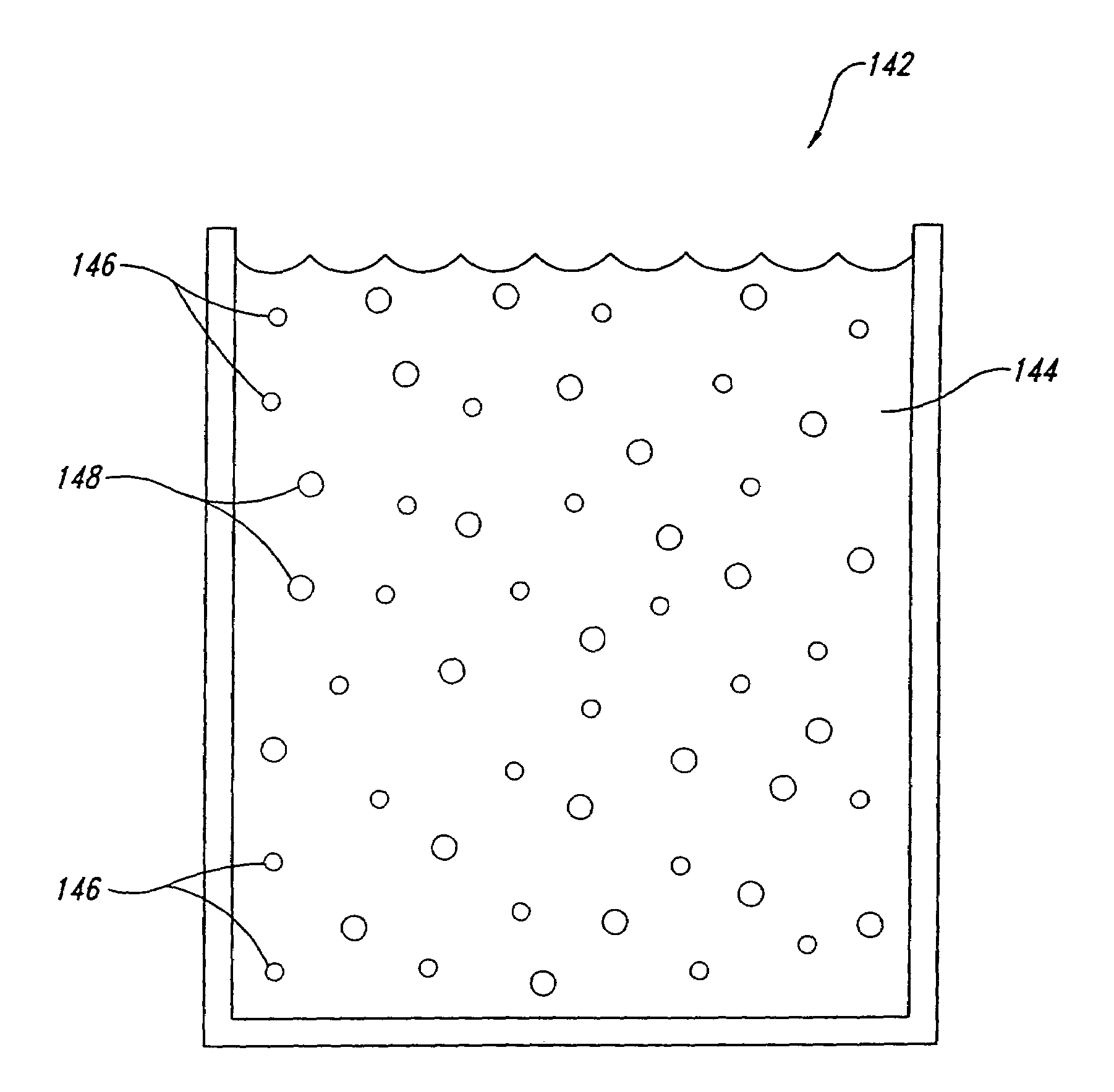
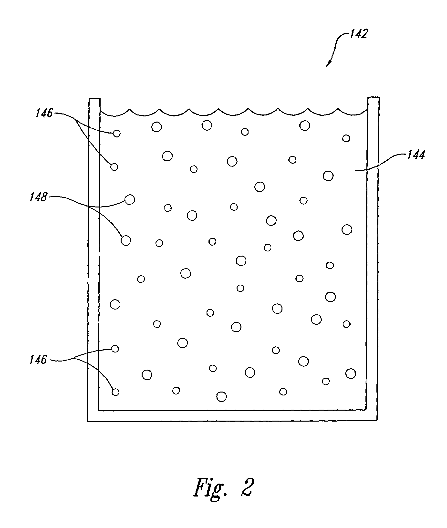
[0028]FIG. 2 is a schematic view of a planarizing solution 142 in accordance with one embodiment of the invention for selectively removing material from a substrate assembly. In this embodiment, the planarizing solution 142 includes a liquid mixture 144, a plurality of first abrasive particles 146, and a plurality of second abrasive particles 148. T...


PUM

PropertyMeasurementUnit
particle size distributionaaaaaaaaaa

Abstract

Planarizing solutions, planarizing machines and methods for planarizing microelectronic-device substrate assemblies using mechanical and / or chemical-mechanical planarizing processes. In one aspect of the invention, a microelectronic-device substrate assembly is planarized by abrading material from the substrate assembly using a plurality of first abrasive particles and removing material from the substrate assembly using a plurality second abrasive particles. The first abrasive particles have a first planarizing attribute, and the second abrasive particles have a second planarizing attribute. The first and second planarizing attributes are different from one another to preferably selectively remove topographical features from substrate assembly and / or selectively remove different types of material at the substrate surface.

Description

CROSS-REFERENCE TO RELATED APPLICATION[0001]This application is a continuation of pending U.S. Pat. application Ser. No. 09 / 706,493, filed Nov. 2, 2000 now U.S. Pat. No. 6,805,615, which is a divisional of U.S. Pat. application Ser. No. 09 / 289,791, filed Apr. 9, 1999, now U.S. Pat. No. 6,599,836.TECHNICAL FIELD[0002]The present invention relates to planarizing solutions, planarizing machines and methods for planarizing microelectronic-device substrate assemblies using mechanical and / or chemical-mechanical planarization processes.BACKGROUND OF THE INVENTION[0003]Mechanical and chemical-mechanical planarizing processes (collectively “CMP”) are used in the manufacturing of microelectronic devices for forming a flat surface on semiconductor wafers, field emission displays and many other microelectronic-device substrate assemblies. CMP processes generally remove material from a substrate assembly to create a highly planar surface at a precise elevation in the layers of material on the su...

Claims


Application Information

Patent Timeline
Patent Type & Authority Patents(United States)
IPC IPC(8): H01L21/461H01L21/302B24B37/04B24B57/02H01L21/321H01L21/768
CPCB24B37/04B24B57/02H01L21/7684H01L21/3212
Inventor ROBINSON, KARL M.MEIKLE, SCOTT G.
Owner MICRON TECH INC
Why Eureka
Try Eureka