Display device using electroluminescence material

a technology of electroluminescence and display device, which is applied in the direction of organic semiconductor devices, semiconductor devices, instruments, etc., can solve the problems of varying the luminous characteristics of the el elements provided in the respective pixels, and achieve the reduction of the manufacturing the reduction of the cost of the electronic device, and the suppression of investment in plant and equipment.

Inactive Publication Date: 2007-10-09
SEMICON ENERGY LAB CO LTD
View PDF29 Cites 74 Cited by
  • Summary
  • Abstract
  • Description
  • Claims
  • Application Information

AI Technical Summary

Benefits of technology

[0008]The present invention has been made in view of the above problem and has an object to provide an electronic device in which fluctuation in the luminescence properties of EL elements among pixels is low and color reproducibility is high. Another object of the present invention is to provide a highly reliable electronic device. Further another object of the present invention is to provide an electronic instrument using the electronic device as a display portion.
[0009]Still another object of the present invention is to provide a process for reducing the manufacturing cost of the electronic device having high color reproducibility described above.
[0012]Moreover, in the present invention, a process of forming a plurality of electronic devices from a large substrate is used to realize a reduction in the manufacturing cost of the electronic device, that is, a reduction of the cost of the electronic device. The present invention is characterized in that the process capable of using the existing liquid crystal line is employed and investment in plant and equipment is suppressed to a minimum, so that a substantial reduction in the manufacturing cost is realized.

Problems solved by technology

However, there has been a problem in that when electrical characteristics of the FETs vary among pixels, luminous characteristics of the EL elements provided in the respective pixels also vary.

Method used


Image

  • Display device using electroluminescence material
  • Display device using electroluminescence material
  • Display device using electroluminescence material

Examples


embodiment 1

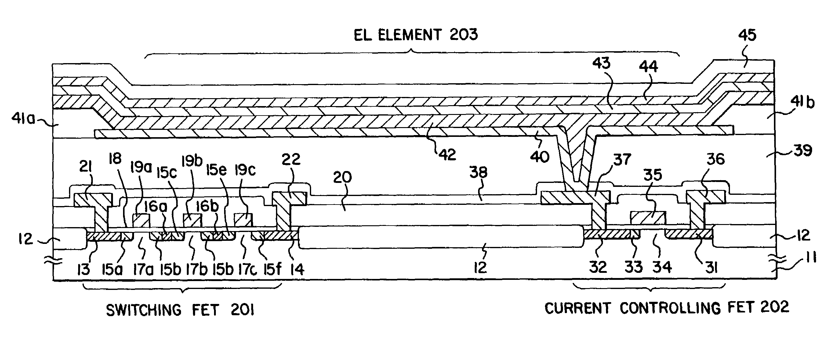
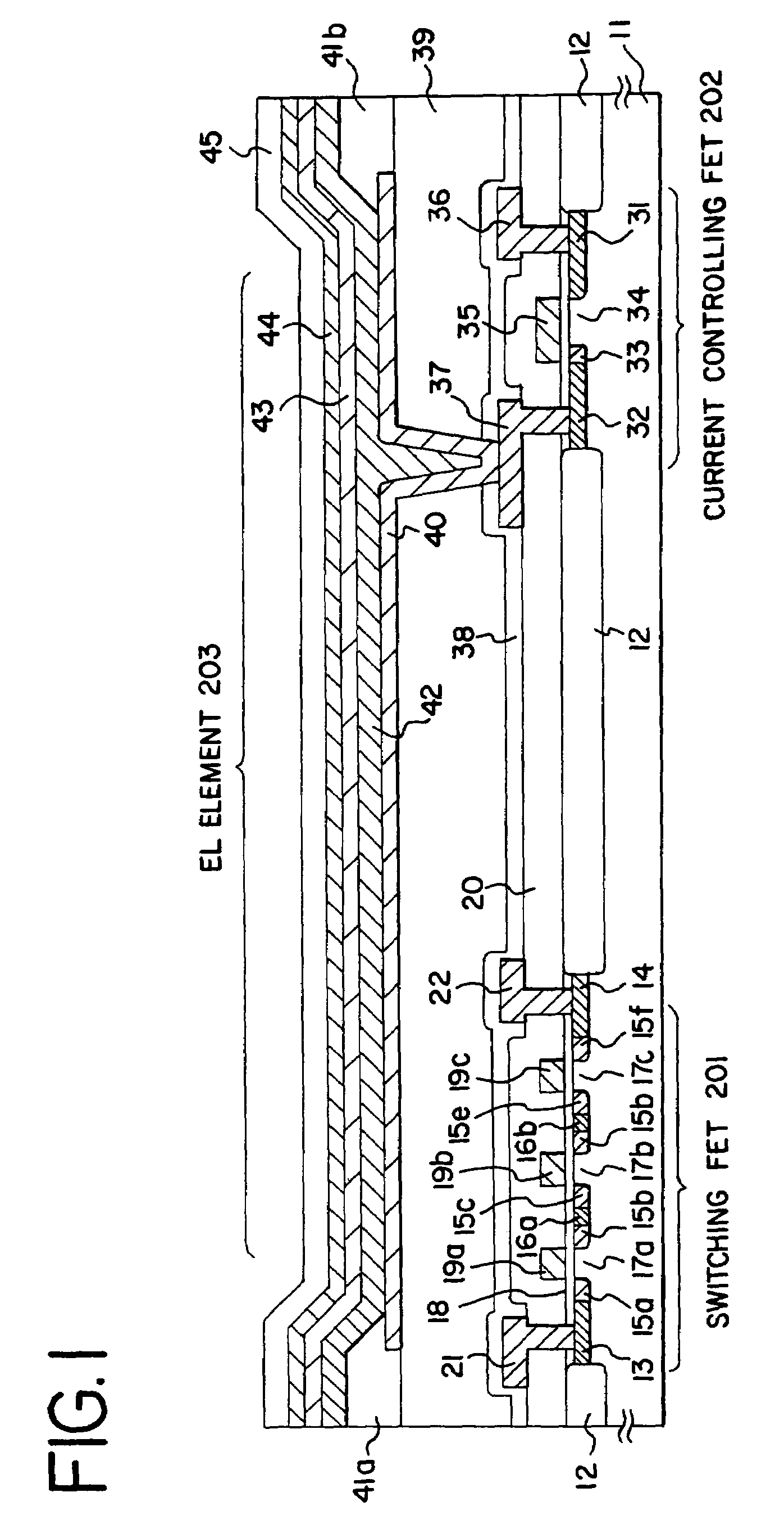
[0070]The embodiments of the present invention are explained using FIGS. 3 to 5. A method of simultaneous manufacture of a pixel portion, and FETs of a driver circuit portion formed in the periphery of the pixel portion, is explained here. Note that in order to simplify the explanation, a CMOS circuit is shown as a basic circuit for the driver circuits.

[0071]First, as shown in FIG. 3A, a field insulating film 302 is formed on the p-type single crystal silicon substrate 300 with a oxide silicon film by well known LOCOS method (local oxidation of silicon). An impurity element which imparts n-type conductivity (hereinafter referred to as an n-type impurity element) is added and n-well 302 is formed. Note that elements residing in periodic table group 15 are generally used as the n-type impurity element, and typically phosphorous or arsenic can be used.

[0072]Next, as shown in FIG. 3B, a protecting film 303 is formed with a silicon oxide film having a thickness of 130 nm. This thickness ...

embodiment 2

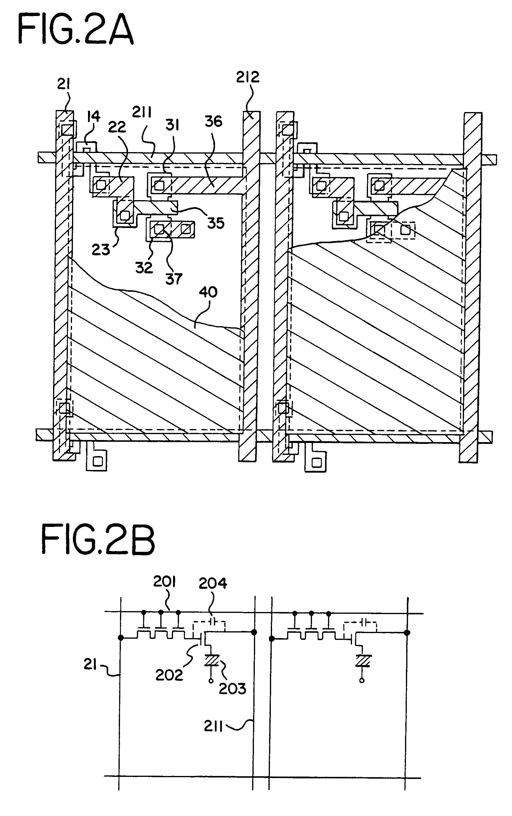
[0127]In this embodiment, an example of a case in which a pixel constitution shown in FIG. 9 differs from that of the circuit diagram (constitution) shown in FIG. 2B. Note that in this embodiment, reference numeral 901 denotes source wiring of a switching FET 902, 903 denotes a gate wiring of a switching FET 902, 904 denotes a current control FET, 905 denotes a capacitor, 906 and 908 denote electric current supply lines, and 907 denotes an EL element.

[0128]It is to be noted that the capacitor 905 employs for maintenance of electric potential of a gate capacitance of the current control FET 904. Substantially, the capacitor 905 is not provided, and therefore it is indicated by a dotted line.

[0129]FIG. 9A is an example of a case in which the electric current supply line 906 is common between two pixels. Namely, this is characterized in that the two pixels are formed having linear symmetry around the electric current supply line 906. In this case, the number of the electric current sup...

embodiment 3

[0133]In this embodiment, examples in which the element structure of the electric current controlling FET 202 shown in FIG. 1 is made a different one, will be described with reference to FIGS. 10A to 10D. Specifically, examples in which the arrangement of the LDD region is made a different one, will be described. Incidentally, the same portions as those of the electric current controlling FET 202 shown in FIG. 1 are designated by the same symbols.

[0134]An electric current controlling FET 202A shown in FIG. 10A is an example in which the LDD region 33 is omitted from the electric current controlling FET 202 shown in FIG. 1. In the case shown in FIG. 1, since the switching FET 201 has a triple-gate structure, an off current value is very small, and if a digital driving system is used, the capacitance of a capacitor for holding the electric potential of the gate of the electric current controlling FET 202A may be very small.

[0135]Thus, as shown in FIG. 10A of this embodiment, it is pos...


PUM


Abstract

There is provided an electronic device having high reliability and high color reproducibility. A pixel structure is made such that a switching FET (201) and an electric current controlling FET (202) are formed on a single crystal semiconductor substrate (11), and an EL element (203) is electrically connected to the electric current controlling FET (202). The fluctuation in characteristics of the electric current controlling FET (202) is very low among pixels, and an image with high color reproducibility can be obtained. By taking hot carrier measures in the electric current controlling FET (202), the electronic device having high reliability can be obtained.

Description

[0001]This application is a continuation of U.S. application Ser. No. 10 / 455,044, filed on Jun. 5, 2003 which is a continuation of U.S. application Ser. No. 09 / 697,069, filed on Oct. 26, 2000, now U.S. Pat. No. 6,580,094 issued Jun. 17, 2003.BACKGROUND OF THE INVENTION[0002]1. Field of the Invention[0003]The present invention relates to an electronic device including an element having a luminous material placed between electrodes and an electronic instrument using the electronic device as a display portion (indication display or indication monitor). Particularly, the present invention relates to an electronic device using a luminous material (hereinafter referred to as EL material) by which EL (Electro Luminescence) is obtained.[0004]2. Description of the Related Art[0005]In recent years, an electronic device (hereinafter referred to as EL display device) which uses a light-emitting device (hereinafter referred to as an EL element) using an EL phenomenon of a luminous material has b...

Claims


Application Information

Patent Timeline
Patent Type & Authority Patents(United States)
IPC IPC(8): H01L27/01H01L27/12H01L31/0392G09G3/30G09G3/32H01L27/32
CPCG09G3/3275H01L27/1203H01L27/3244H01L27/3262G09G3/3233G09G3/30H01L2251/566G09G2300/0426G09G2300/0465G09G2300/0809G09G2300/0842G09G2310/061G09G2320/0233H01L29/66772H01L29/78621H10K59/12H10K59/1213H10K71/851
Inventor YAMAZAKI, SHUNPEIKONUMA, TOSHIMITSUKOYAMA, JUNINUKAI, KAZUTAKAMIZUKAMI, MAYUMI
Owner SEMICON ENERGY LAB CO LTD
Why Eureka
Try Eureka