
Stacked semiconductor device and semiconductor memory module

a semiconductor memory module and semiconductor technology, applied in the field of stackable semiconductor devices and semiconductor memory modules, can solve the problems of easy deterioration of waveforms by large ringing, and achieve the effect of preventing the deterioration of signal waveforms and reducing ringing

Inactive Publication Date: 2007-10-16
LONGITUDE LICENSING LTD
View PDF11 Cites 26 Cited by
  • Summary
  • Abstract
  • Description
  • Claims
  • Application Information

AI Technical Summary

Benefits of technology

[0014]An object of the present invention is to provide a stacked semiconductor device and a semiconductor device module in which a signal waveform is not greatly deteriorated even in a high-speed signal transmission.
[0033]According to the present invention, it is possible to provide a stacked semiconductor device and a semiconductor memory module capable of reducing ringing due to signal reflection easily generated in a high-speed transmission system and preventing the signal waveform from deteriorating.

Problems solved by technology

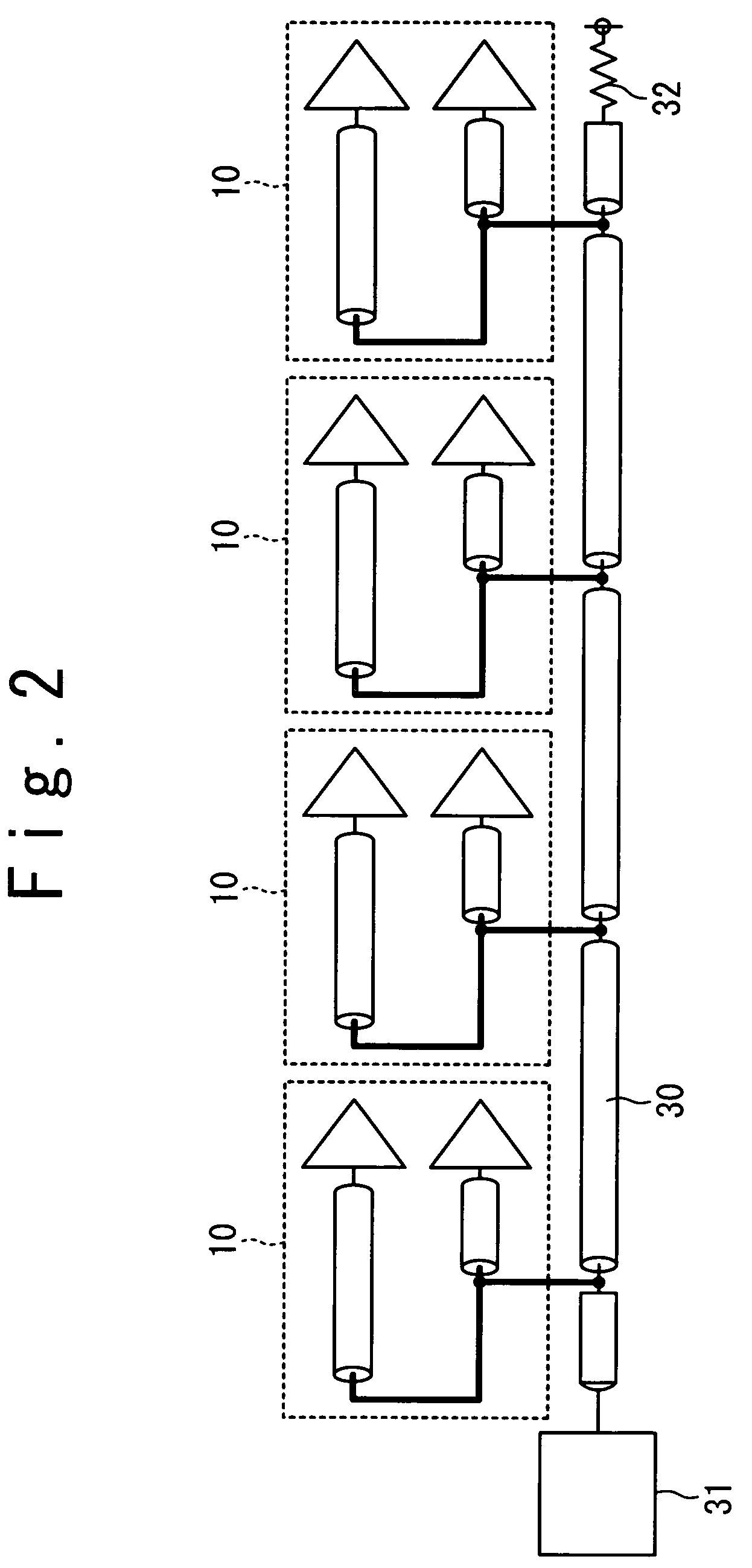
Specifically, the stacked memory 10 closest to the controller 31 has a problem that the rising of a waveform is steep, so that large ringing easily occurs to deteriorate the waveform.

Method used


Image

  • Stacked semiconductor device and semiconductor memory module
  • Stacked semiconductor device and semiconductor memory module
  • Stacked semiconductor device and semiconductor memory module

Examples


first embodiment

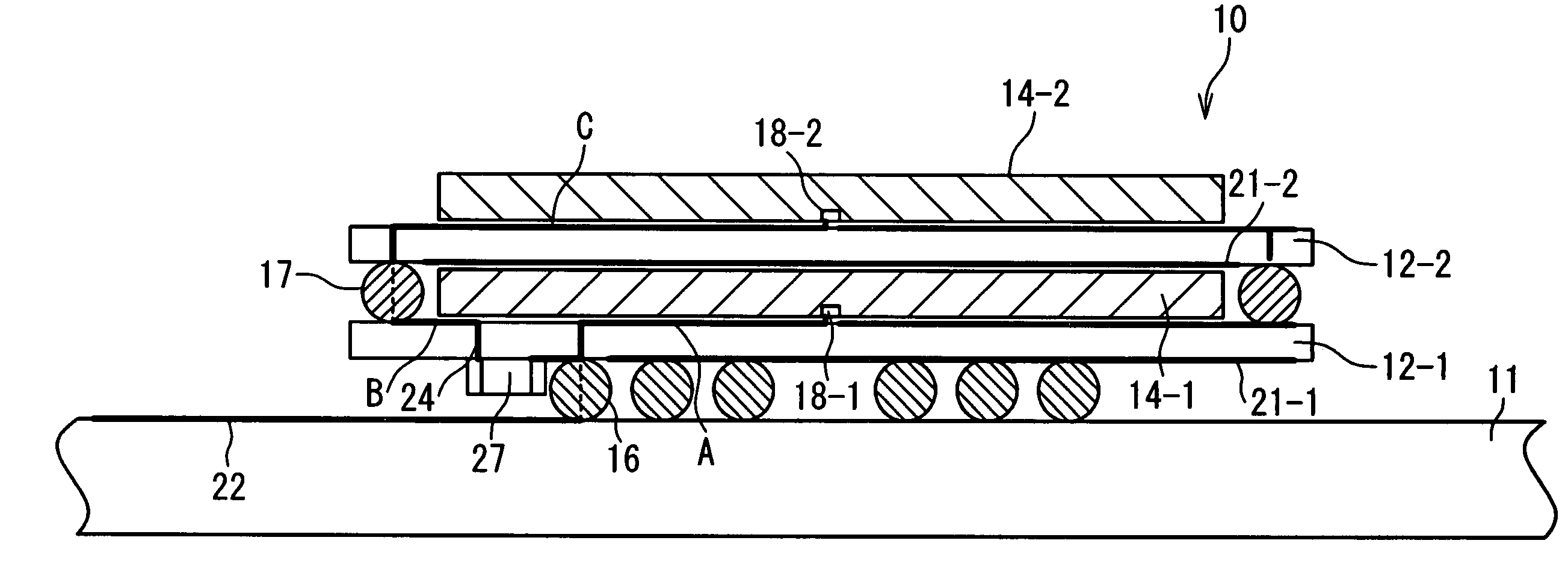
[0059]FIGS. 3A and 3B show a configuration of a stacked memory as the stacked semiconductor device used for a memory module as the semiconductor device module according to the present invention. As shown in FIG. 3A, the stacked memory 10 is mounted on a memory module substrate (PCB) 11 through package terminals as ball terminals 16 of a BGA (Ball Grid Array) structure. Thus, the stacked memory 10 is connected with the memory module substrate 11 are connected by the package terminals 16. In case of the stacked memory 10, a package substrate 12-2 for mounting the memory chip 14-2 is stacked on the package substrate 12-1 for mounting the memory chip 14-1. The package substrate 12-1 is electrically connected with the memory chip 14-1, and the package substrate 12-2 is electrically connected with the memory chip 14-2. Each of the package substrates 12-1 and 12-2 has a 2-layer metal structure in which an insulating layer is put between metal layers. The surface wiring patterns of the pack...

second embodiment

[0082]In the stacked memory 10 of the second embodiment, the package substrate 12-2 for mounting the memory chip 14-2 is stacked on the package substrate 12-1 for mounting the memory chip 14-1. The package substrates 12-1 and 12-2 are connected to each other through the connection balls 17 arranged their right and left ends. The lowermost package substrate 12-1 has the package terminals 16 of the BGA structure and is connected to the memory module substrate 11. In this case, the substrates 12-1 and 12-2 are connected through the connection balls 17. However, another method may be employed in which these substrate 12-1 and 12-2 are electrically connected.

[0083]The package substrate 12 has the two-layer metal structure and the signal wiring has a transmission line structure by using the ground layer. Portions other than signal wirings and openings are covered with the ground layer 21 on the lower surface of the package substrate 12, so that a signal characteristic is stabilized. Signa...

third embodiment

[0092]FIGS. 15A and 15B show a configuration of the stacked memory 10 mounted on the memory module according to the present invention. As shown in FIG. 15A, the stacked memory 10 is arranged on the memory module substrate 11 and a wiring in the stacked memory 10 and the signal wiring 22 on the memory module substrate 11 are connected by the ball terminal 16. The ball terminal 16 is of the BGA type.

[0093]In the stacked memory 10, the package substrate 12-1 for mounting the memory chip 14-2 is stacked on the package substrate 12-1 for mounting the memory chip 14-1. The package substrate 12-1 and 12-2 are connected by the connection balls 17 which are arranged at the right and left sides the substrates. The lower-stage package substrate 12-1 has the package terminals 16 of the BGA type which are connected to the signal lines on the memory module substrate 11. In this case, substrates 12-1 and 12-2 are connected through the connection balls 17. However, another method may be used as lon...


PUM


Abstract

A semiconductor device module includes a wiring substrate, a plurality of stacked semiconductor devices and a damping impedance circuit. The plurality of stacked semiconductor devices are provided on the wiring substrate and connected with a signal in a stubless manner, and each of the plurality of stacked semiconductor devices comprises a plurality of semiconductor chips which are stacked. The damping impedance circuit is provided for a transmission path of the signal for an uppermost semiconductor chip as the furthest one, from the wiring substrate, of the plurality of semiconductor chips of a first stacked semiconductor device as one of the plurality of stacked semiconductor devices which is first supplied with the signal.

Description

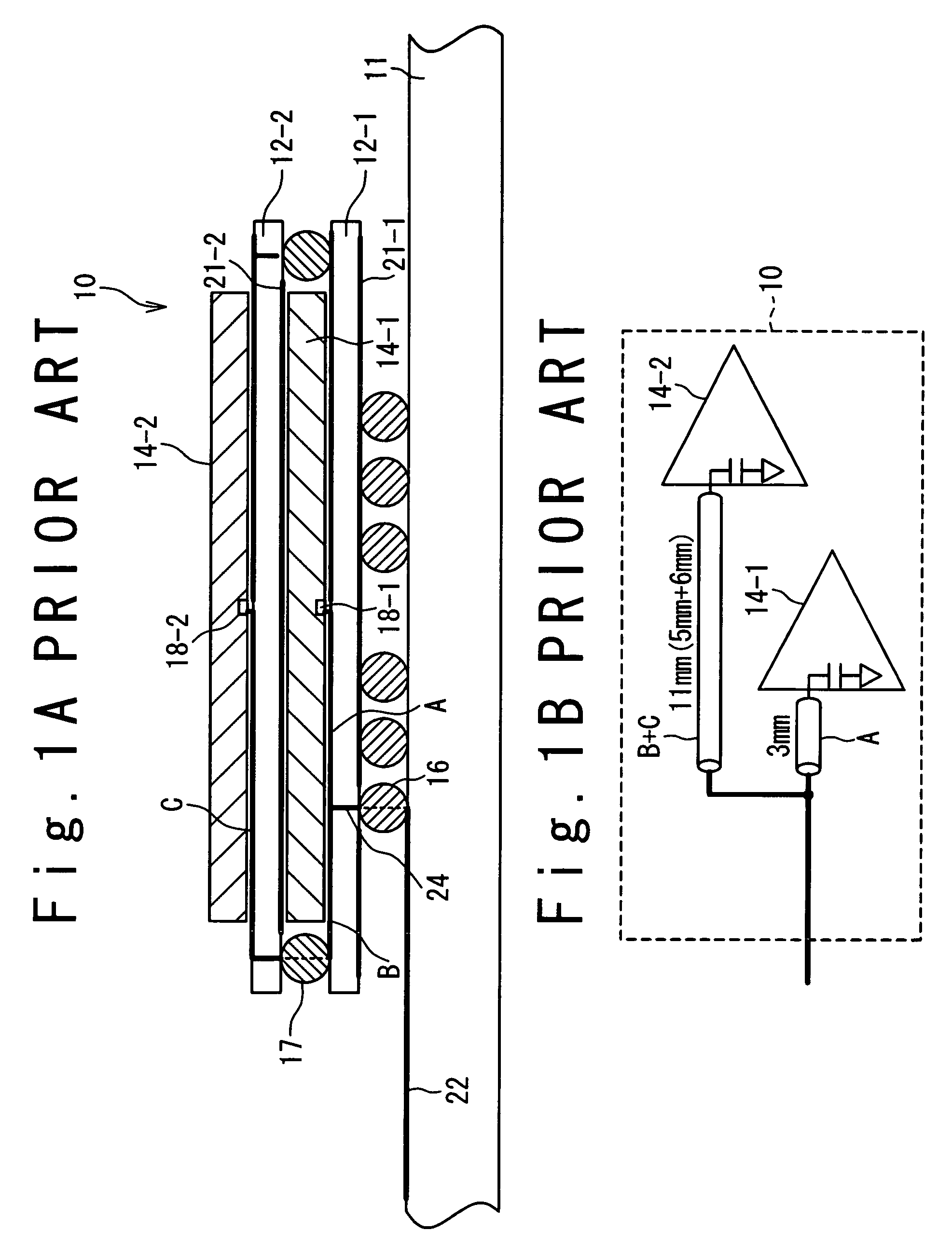
BACKGROUND OF THE INVENTION[0001]1. Field of the Invention[0002]The present invention relates to a stacked semiconductor device and a semiconductor device module, particularly to a stacked semiconductor device and a semiconductor memory module used for a high-speed signal transmission system.[0003]2. Description of the Related Art[0004]FIGS. 1A and 1B are diagrams showing a structure of a conventional stacked memory as a stacked semiconductor device. As shown in FIG. 1A, a stacked memory 10 has the structure in which package substrates (tapes) 12 (12-1 and 12-2) mounting memory chips 14 (14-1, 14-2) are stacked through connecting balls 17 arranged at the both sides of the package substrates 12. A lower-stage package substrate 12-1 has a BGA (Ball Grid Array) structure. Moreover, the package substrate 12 has a structure of two metal layers, and a signal wiring has a same structure as a transmission line. A signal wiring 22 on a memory module substrate (PCB) 11 is connected with a sig...

Claims


Application Information

Patent Timeline
Patent Type & Authority Patents(United States)
IPC IPC(8): H01L23/02
CPCG11C5/04G11C5/063H01L23/66H01L24/06H01L25/0657H01L2924/13091H01L2224/0401H01L2224/04042H01L2224/06136H01L2224/49171H01L2225/06527H01L2924/01082H01L2924/014H01L2924/15311H01L2924/15331H01L2924/19041H01L2924/19105H01L2924/19106H01L2924/3011H01L24/49H01L2924/01005H01L2924/01006H01L2924/01023H01L2924/01033H01L2924/00H01L2224/05553H01L2224/05554H01L2224/0603H01L2924/00014H01L2224/45099H01L2224/45015H01L2924/207
Inventor FUNABA, SEIJINISHIO, YOJI
Owner LONGITUDE LICENSING LTD
Learn More