Eight transistor SRAM cell with improved stability requiring only one word line

a sram cell, eight transistor technology, applied in static storage, information storage, digital storage, etc., can solve the problems of reducing the stability of the sram cell, the degree to which the device channel parameters can be controlled, and the decrease of the cell performance. achieve the effect of reducing the cell area requirements without affecting the writing speed

Inactive Publication Date: 2007-11-13
GLOBALFOUNDRIES INC
View PDF6 Cites 7 Cited by
  • Summary
  • Abstract
  • Description
  • Claims
  • Application Information

AI Technical Summary

Benefits of technology

[0012]An object of this invention is the provision of an improved SRAM cell that provides cell stability, with reduced cell area requirements without impacting the writing speed to the cell.

Problems solved by technology

However a higher beta ratio results in decreased cell performance, such as slower write.
Particularly, sub 100 nm silicon technologies are having increased problems with cell SRAM cell stability when trying to write to the cells at high rates due to the inherent variations in individual cell beta ratios as a result to limitations in the degree to which device channel parameters can be controlled at these extremely small devices sizes.
However these prior art proposals have not proven satisfactory.

Method used


Image

  • Eight transistor SRAM cell with improved stability requiring only one word line
  • Eight transistor SRAM cell with improved stability requiring only one word line
  • Eight transistor SRAM cell with improved stability requiring only one word line

Examples


Embodiment Construction

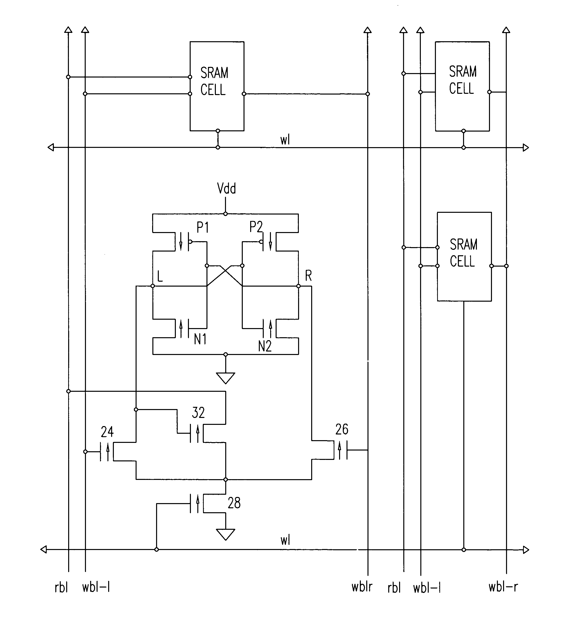
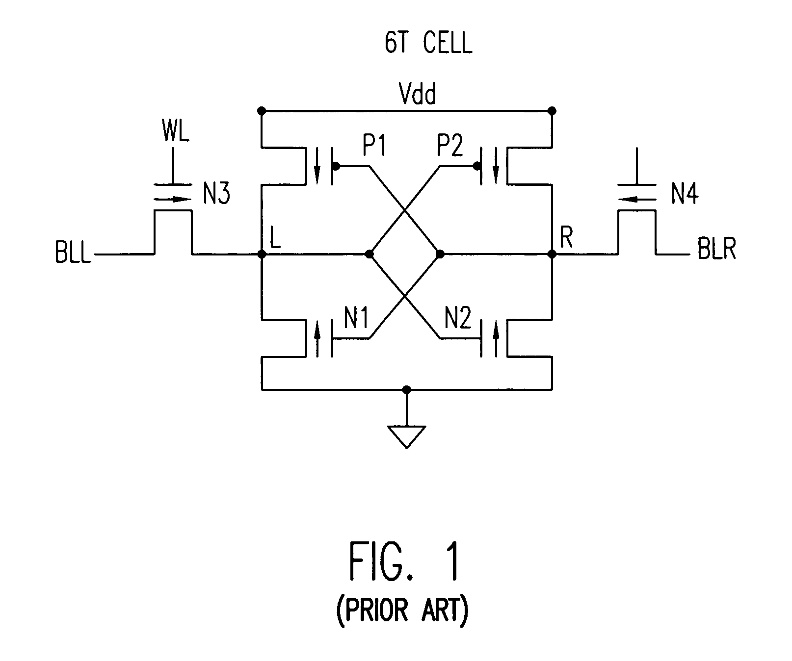
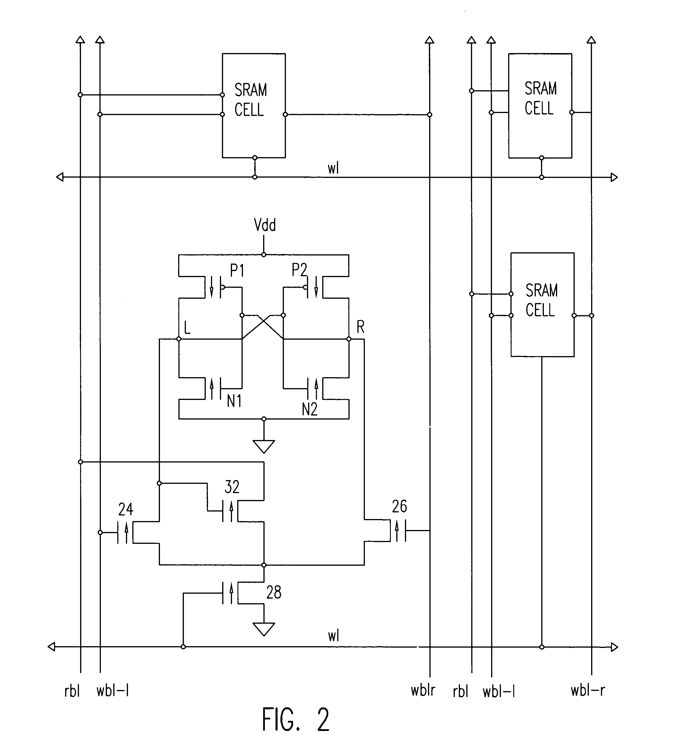
[0019]Referring now to FIG. 2 of the drawings, the part of the cell comprised of PFET pull-up transistors P1 and P2 and NFET pull-down transistors N1 and N2 connected to nodes R and L is the same as the corresponding part of the prior art cell discussed above, where like reference numbers are used, and will not be further explained here. In accordance with the teachings of this invention, a pair of NFET write access transistors 24 and 26 provides access to the nodes R and L in a write operation. The source of the left hand NFET 24 is connected to the left node L and the source of the right hand NFET 26 is connected to the right node R. The drains of NFET 24 and 26 are connected to ground (i.e. common) via a word line NFET 28 whose source is connected to the drains of NFET 24 and 26 and whose drain is connected to ground. The gate of the left write access NFET 24 is connected to a normally low left write bit line wbl_l and the gate of the right write access NFET 26 is connected to a ...


PUM


Abstract

An SRAM cell that is accessed by a single word line and separate access transistors for read and write operations. A pair of write bit line transfer devices provide respectively access to the right and left sides of cross coupled pull-up, pull-down transistor pairs for a write operation, and a single read bit line transistor in series with the word line transistor, when selected, reads the content of the cell.

Description

CROSS-REFERENCE TO RELATED APPLICATIONS[0001]This application contains subject matter that is related to the subject matter of the following co-pending applications, each of which is assigned to the same assignee as this application, International Business Machines Corporation of Armonk, N.Y. Each of the below listed applications is hereby incorporated herein by reference in its entirety.TRADEMARKS[0002]IBM® is a registered trademark of International Business Machines Corporation, Armonk, N.Y., U.S.A. S / 390, Z900 and z990 and other names used herein may be registered trademarks, trademarks or product names of International Business Machines CorporationBACKGROUND OF THE INVENTION[0003]1. Field of the Invention[0004]This invention relates to an improved Static Random Access Memory (SRAM) cell and more particularly to stable cell with only one word line.[0005]2. Description of the Background[0006]Typical prior art CMOS SRAM cells have a six-transistor typology, such as that shown in FI...

Claims


Application Information

Patent Timeline
Patent Type & Authority Patents(United States)
IPC IPC(8): G11C11/00
CPCG11C11/412G11C8/14
Inventor CHAN, YUEN H.HUOTT, WILLIAM V.PLASS, DONALD W.
Owner GLOBALFOUNDRIES INC
Why Eureka
Try Eureka