Integrated circuit memory with write assist

a write assist and circuit memory technology, applied in the field of integrated circuit memory, can solve the problems of slow switching between these two power supplies, inability to quickly switch from writing a memory cell to and inability to quickly switch between writing a memory cell and reading that same memory cell. , to achieve the effect of convenient switching, effective weakening the power supply to the memory cell, and facilitating the writing of new data values

Active Publication Date: 2008-01-29
ARM LTD
View PDF4 Cites 41 Cited by
  • Summary
  • Abstract
  • Description
  • Claims
  • Application Information

AI Technical Summary

Benefits of technology

[0011]when writing to said at least one memory cell said power supply control circuit provides a high resistance path, with a resistance greater than said low resistance path, between said supply input and said supply output so that said at least one memory cell is more readily switched between said first state and said second state.
[0012]In accordance with the present technique a memory cell is provided with power via a power supply control circuit including at least two gates which are switched by a write assist signal to provide either a low resistance or high resistance path through the power supply control circuit. Thus, the memory cell is always powered and connected to the power supply, but when the high resistance path is in use during writing to the memory cell, then this will effectively weaken the power supply to the memory cell such that it is easier for a new data value being written into that memory cell, i.e. to change the state of the memory cell and overcome the inherent stability in the memory cell which tends to oppose changes in its state. This technique does not require separate power supply lines to be routed through the memory structure and does not leave the memory cell isolated from the power supply in a way which renders it vulnerable to inadvertent data loss.
[0013]It will be appreciated that the first gate and the second gate within the power supply control circuit could be controlled in a variety of different ways by the write assist signal. A preferred way of controlling the first and second gates is that the first gate is switched to a conductive state by the write assist signal when not writing to the memory cell and is switched to a non-conductive state by the write assist signal when writing to the memory cell. Thus, whatever contribution is being made to the strength of the power supply to the memory cell by current passing through the first gate, this is removed when writing to the memory cell. The second gate can be permanently conductive and supply a relatively weak power supply to the memory cell during writing such that the memory cell will not inadvertently lose data if it is not actually being written to and yet will less strongly resist changes in its state due to a new value being written therein.

Problems solved by technology

A disadvantage with this approach is that two separate power rails need to be routed through the memory, which uses a disadvantageous amount of space.
Furthermore, the switching between these two power supplies is relatively slow such that it is difficult to rapidly switch from writing a memory cell to reading that same memory cell or a memory cell connected to the same power supply.
Memory cells are not normally provided with individually controllable power supplies since this would consume a disadvantageous number of gates and reduce the memory density.
However, when multiple memory cells share a power supply in this way, all of these memory cells will be isolated from the power supply and be unpowered whilst one of the memory cells is being written.
This will leave the unpowered memory cells vulnerable to data loss.
This risk is increased when one considers manufacturing and process variations which can occur rendering individual memory cells particularly vulnerable to data loss when unpowered.
This approach suffers from the disadvantage of potentially rendering a memory unreliable.

Method used


Image

  • Integrated circuit memory with write assist
  • Integrated circuit memory with write assist
  • Integrated circuit memory with write assist

Examples


Embodiment Construction

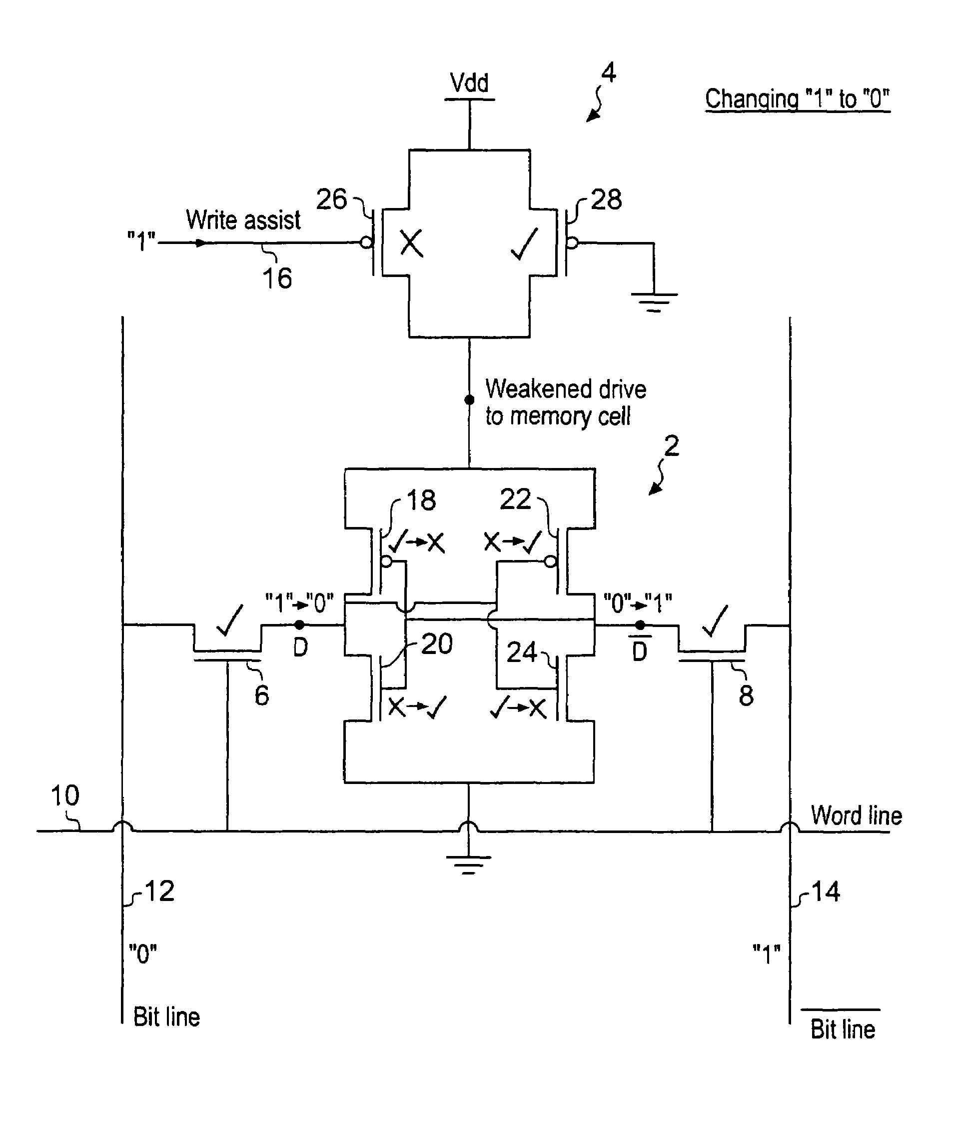
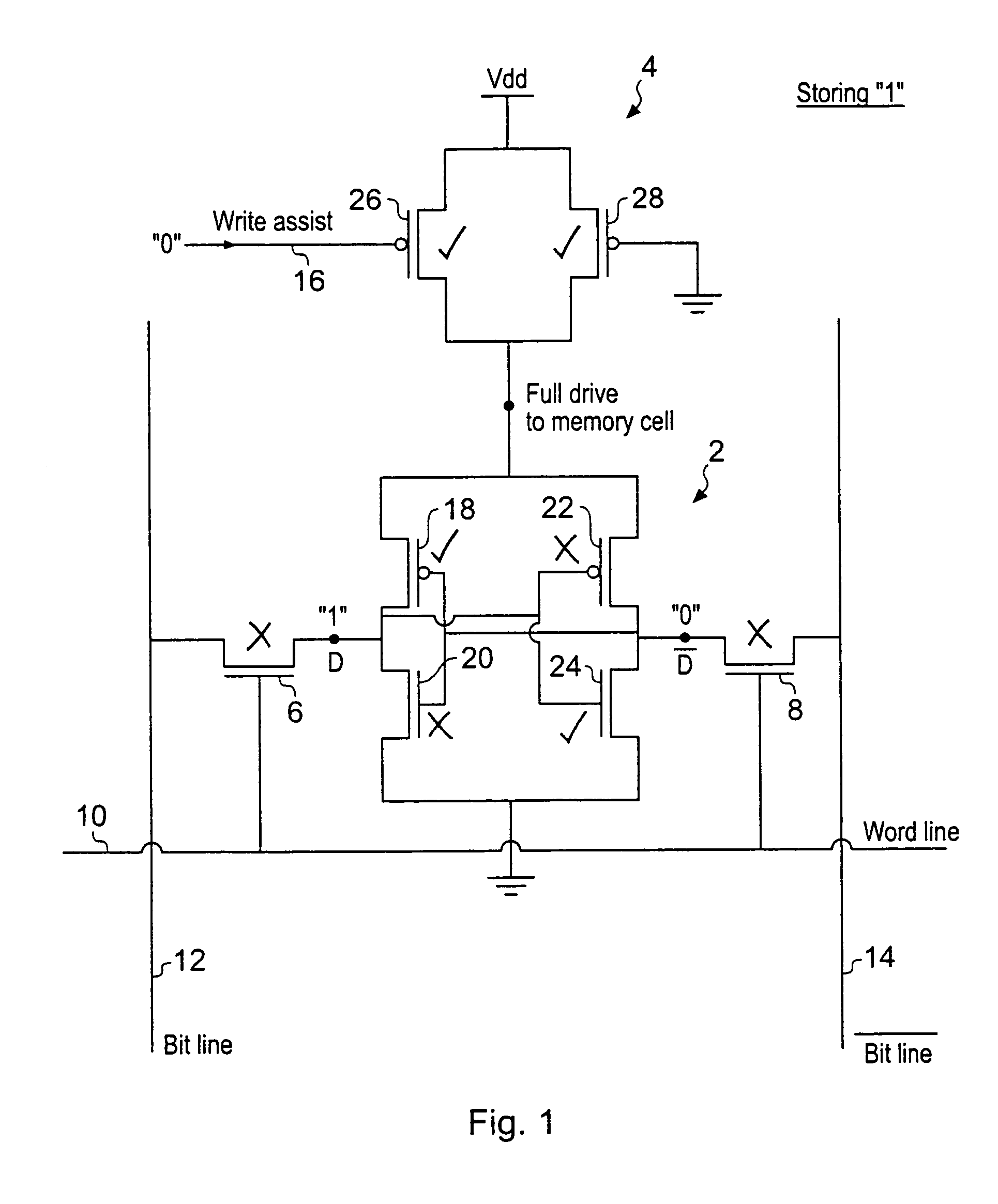
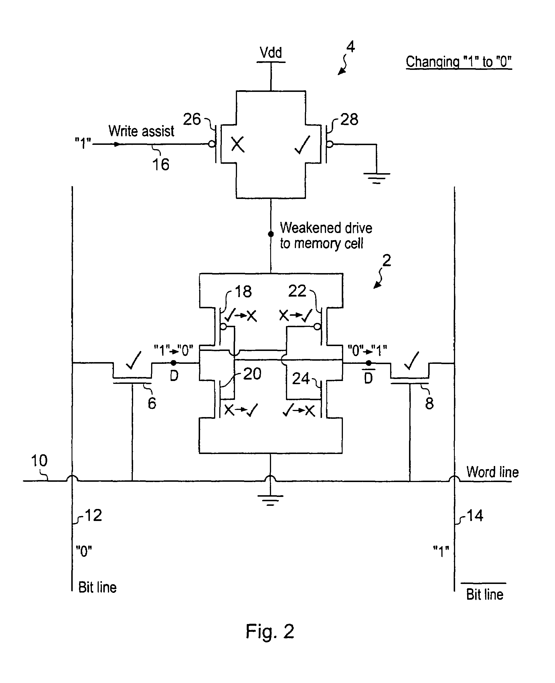
[0029]FIG. 1 illustrates a portion of an integrated circuit memory comprising a memory cell 2, a power supply control circuit 4, pass gates 6, 8, a word line 10, bit lines 12, 14 and a write assist line 16. The memory cell 2 comprises a pair of cross-coupled inverters formed by transistors 18, 20, 22 and 24. The power supply control circuit 4 comprises a first gate 26. The first gate 26 is switched by the write assist signal on the write assist signal line 16 to be conductive when the memory cell 2 is not being written and to be non-conductive when the memory cell 2 is being written. A second gate 28 is permanently conductive and provides power to the memory cell 2 both when the memory cell 2 is being written and when the memory cell 2 is not being written.

[0030]The first gate 26 is a physically larger gate than the second gate 28 and accordingly provides a low(er) resistance path between the power supply Vdd and the memory cell 2. The second gate 28 is physically smaller and is onl...


PUM


Abstract

An integrated circuit memory includes memory cells 2 is connected to a power supply Vdd via a power supply control circuit 4. The power supply control circuit includes a first gate 26 and a second gate 28. The first gate 26 is switched by a write assist circuit so as to be non-conductive when writing to the memory cell 2. The second gate 28 is conductive both when writing to the memory cell 2 and when not writing to the memory cell 2. Accordingly, when a write operation is made a relatively high resistance path is formed through the power supply control circuit 4 compared to when writing is not being performed. This increase in the resistance through the power supply control circuit 4 during write operations induces a dip in the virtual supply voltage provided at the supply output of the power supply control circuit 4 in a manner which assist writes to be made. If individual memory cells 2 tend to resist changes in their state more strongly, then they will tend to draw more current which will in turn result in a larger virtual supply voltage dip which will assist more strongly in encouraging those memory cells 2 to change state.

Description

BACKGROUND OF THE INVENTION[0001]1. Field of the Invention[0002]This invention relates to the field of integrated circuit memories. More particularly, this invention relates to write assist mechanisms for use within integrated circuit memories to allow data values to be more readily written.[0003]2. Description of the Prior Art[0004]It is known to provide integrated circuit memories with write assist mechanisms to enable data values to be more readily written to the memory cells. One known system uses two power supply rails connected by respective gates to each memory cell to be written. A first of these power supplies is used to power the memory cell in modes other than a write mode and utilises a relatively high supply voltage level. The second power supply has a lower voltage level and is used during write operations to power the memory cell. The lower supply voltage used during such write operations enables the memory cell to be more readily written. A disadvantage with this app...

Claims


Application Information

Patent Timeline
Patent Type & Authority Patents(United States)
IPC IPC(8): G11C11/00
CPCG11C11/419
Inventor WANG, KARL LINGAJJEWAR, HEMANGI UMAKANT
Owner ARM LTD
Why Eureka
Try Eureka