Organic EL display and active matrix substrate
an organic el and substrate technology, applied in the field of display and array substrates, can solve the problems of difficult image display corresponding to written video signals, and achieve the effect of increasing the display quality of an active matrix organic el display
- Summary
- Abstract
- Description
- Claims
- Application Information
AI Technical Summary
Benefits of technology
Problems solved by technology
Method used
Image

Examples
first embodiment
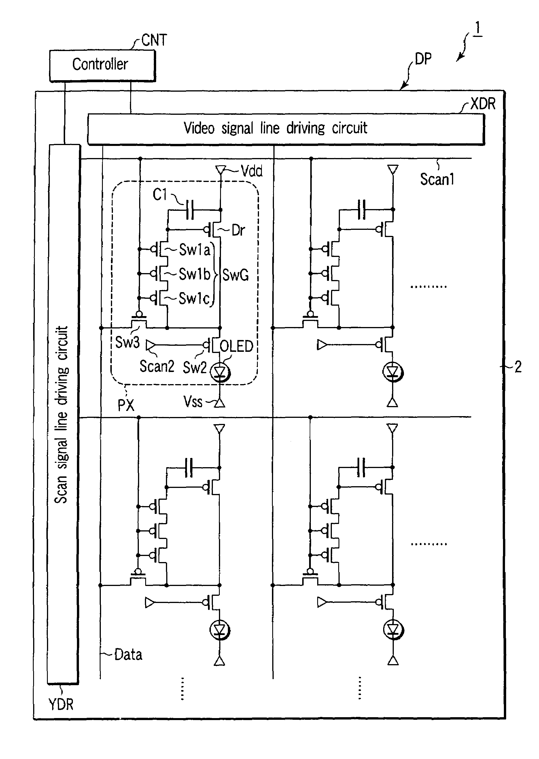
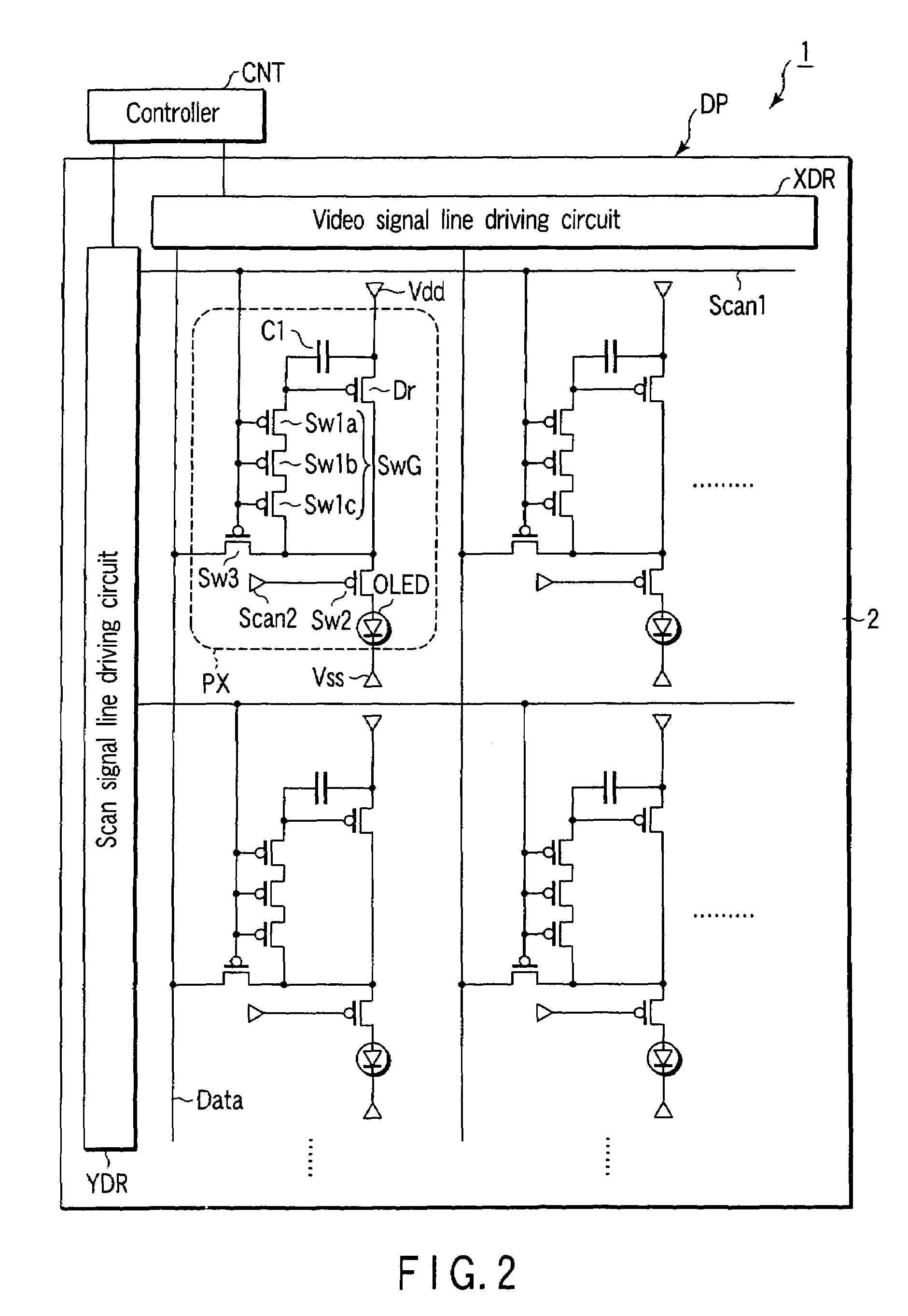
[0045]FIG. 2 is a plan view schematically showing an active matrix organic EL display according to the present invention.
[0046]An active matrix organic EL display 1 shown in FIG. 2 includes an organic EL panel DP and a controller CNT.
[0047]The organic EL panel DP includes an insulating substrate 2 such as a glass substrate. Pixels PX are arrayed in a matrix on one major surface of the substrate 2. The pixels PX define a display region on the major surface of the substrate 2. A scan signal line driver YDR and video signal line driver XDR as driving circuits are arranged in a region outside the display region, i.e., in the peripheral region.
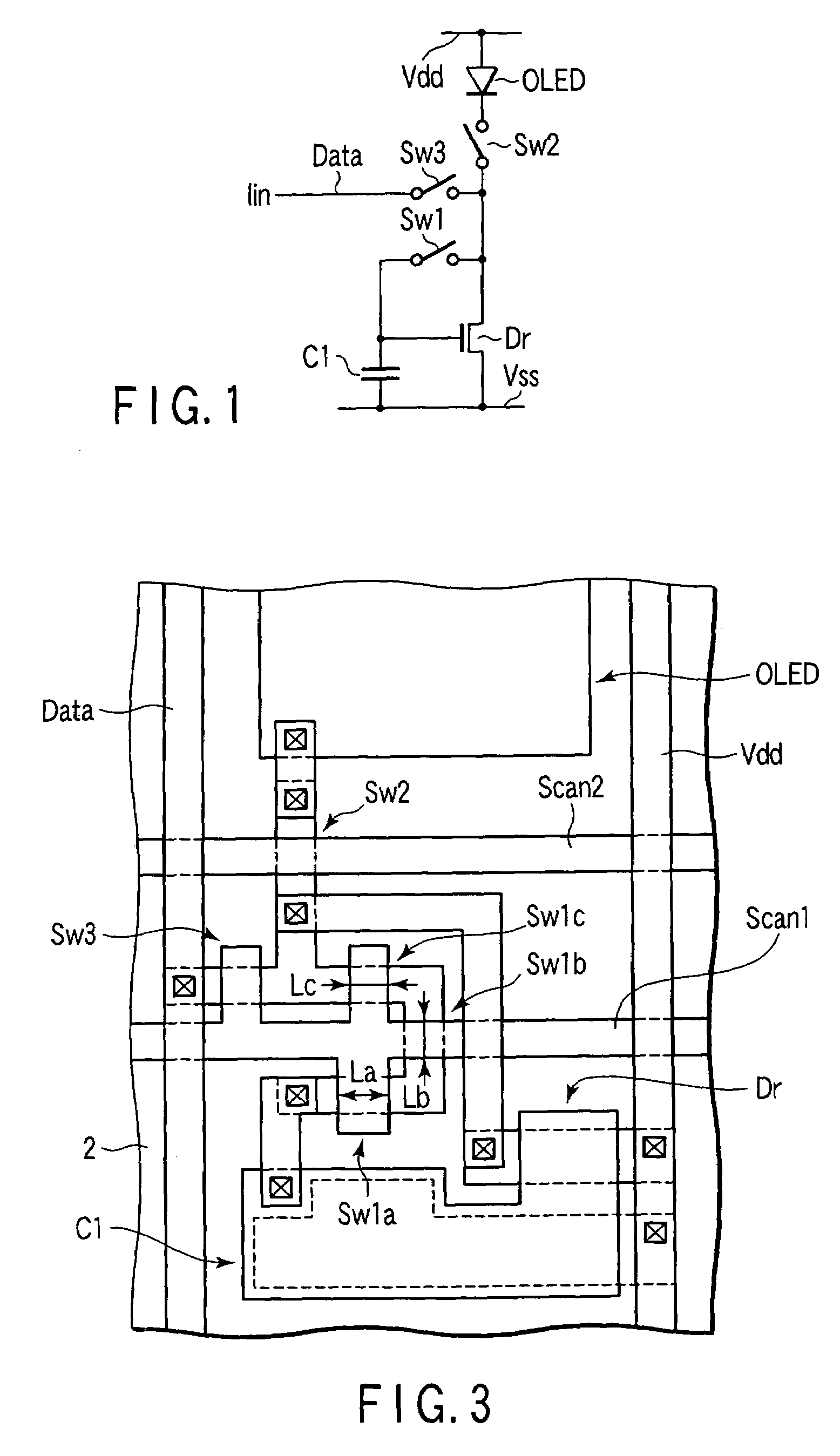
[0048]Each pixel PX includes an organic EL element OLED, a drive control element Dr, a capacitor C1, a switch group SwG formed by connecting a plurality of switches in series, a switch Sw2, and a switch Sw3. As an example, the switch group SwG includes three switches Sw1a to Sw1c. As an example, p-channel TFTs (thin-film transistors) as a kind of f...
second embodiment
[0089]the present invention will be described next.
[0090]In the first embodiment, by controlling the threshold values in the switch group SwG, of the switches Sw1a to Sw1c included in the switch group SwG, the switch Sw1a located on the gate side of the drive control element Dr is controlled to be turned off earlier than the remaining switches Sw1b and Sw1c. In the second embodiment, the same effect as in the first embodiment is achieved by controlling the waveform of the scan signal to be supplied to a switch group SwG.
[0091]FIG. 8 is a plan view schematically showing an organic EL display according to the second embodiment of the present invention. FIG. 9 is an equivalent circuit diagram showing an example of a pixel circuit which can be employed in the organic EL display shown in FIG. 8. Referring to FIG. 8, reference symbol AA denotes a display region.
[0092]In an organic EL display 1 according to the second embodiment, each pixel PX has a delay element Dly which delays and outpu...
third embodiment
[0130]FIG. 16 is an equivalent circuit diagram showing an example of a pixel circuit which can be employed in an active matrix organic EL display according to the present invention. The pixel PX includes an organic EL element OLED, a drive control element Dr, a capacitor C1, a capacitor C2, a delay element Dly, a switch group SwG formed by connecting a plurality of switches in series, a switch Sw2, and a switch Sw3. As an example, the switch group SwG includes three switches Sw1a to Sw1c. As an example, p-channel TFTs are used as the drive control element Dr, switches Sw1a to Sw1c, switch Sw2, and switch Sw3.
[0131]The drive control element Dr, switch Sw2, and organic EL element OLED are connected in this order in series between a power supply line Vdd and a power supply line Vss.
[0132]A terminal of the capacitor C1 is connected to the control terminal of the drive control element Dr. The capacitor C1 holds the potential difference between the gate and source of the drive control ele...
PUM
 Abstract
Description
Claims
Application Information
 - R&D
- Intellectual Property
- Life Sciences
- Materials
- Tech Scout
- Unparalleled Data Quality
- Higher Quality Content
- 60% Fewer Hallucinations
Browse by: Latest US Patents, China's latest patents, Technical Efficacy Thesaurus, Application Domain, Technology Topic, Popular Technical Reports.
© 2025 PatSnap. All rights reserved.Legal|Privacy policy|Modern Slavery Act Transparency Statement|Sitemap|About US| Contact US: help@patsnap.com