High frequency package, transmitting and receiving module and wireless equipment

a high-frequency package and receiver technology, applied in the direction of using reradiation, instruments, printed circuit non-printed electric components association, etc., can solve the problems of difficult to satisfy the desired electromagnetic interference (emi) characteristic, expensive casings and the like, etc., to reduce manufacturing costs, suppress the passage of high-frequency components, and suppress leakage of high-frequency components to the outside of high-frequency packages.

Active Publication Date: 2008-02-26
MITSUBISHI ELECTRIC CORP
View PDF12 Cites 37 Cited by
  • Summary
  • Abstract
  • Description
  • Claims
  • Application Information

AI Technical Summary

Benefits of technology

[0015]According to the present invention, a resistance film is provided on at least one of the upper surface and the lower surface of the internal-layer signal line through which the bias and control signal is transmitted. Therefore, a resistive element absorbs the high-frequency signal coupled to the internal-layer signal line, based on the skin effect, and a bias voltage or a control signal can be transmitted without a voltage drop. Accordingly, based on a low-cost configuration, the high-frequency signal can be suppressed from being discharged to the outside of the high-frequency package through the signal via, the internal-layer signal line, and the external terminal.
[0016]According to the next invention, a slot line having a length of approximately a quarter of an effective wavelength of a high-frequency signal used in-a high-frequency semiconductor is provided on an internal-layer signal line for a bias and control signal. With this arrangement, a high-frequency component that enters a multilayer dielectric substrate is reflected at the position of the slot line, thereby suppressing passage of the high-frequency component to an external terminal. Therefore, leakage of a high-frequency component to the outside of the high-frequency package can be securely suppressed. Since the leakage of the high-frequency component to the outside of the high-frequency package can be suppressed inside the high-frequency package, manufacturing cost can be decreased.
[0017]According to the next invention, a distance between a first ground via string and a second ground via string is set to less than a half of an effective wavelength of a high-frequency signal used in a high-frequency semiconductor. With this arrangement, entrance of a high-frequency component to a direction along the ground via within the multilayer dielectric substrate can be suppressed. Since the distance between the first ground via string and the second ground via string is set to less than a half of the effective wavelength of a high-frequency signal used in the high-frequency semiconductor, entrance of a high-frequency component to a direction perpendicular to the ground via string within the multilayer dielectric substrate is also suppressed. Therefore, according to the present invention, a coupling of a high-frequency signal to the signal via within the multilayer dielectric substrate or to the internal-layer signal line can be suppressed. Further, discharging of an unnecessary wave to the outside of the high-frequency package via the signal via, the internal-layer signal line, and the external terminal can be suppressed.

Problems solved by technology

Therefore, it is very difficult to satisfy a desired electromagnetic interference (EMI) characteristic.
However, when such a configuration that the transmission / reception module is covered with the metallic cover is applied, an expensive casing and the like are necessary.

Method used


Image

  • High frequency package, transmitting and receiving module and wireless equipment
  • High frequency package, transmitting and receiving module and wireless equipment
  • High frequency package, transmitting and receiving module and wireless equipment

Examples


first embodiment

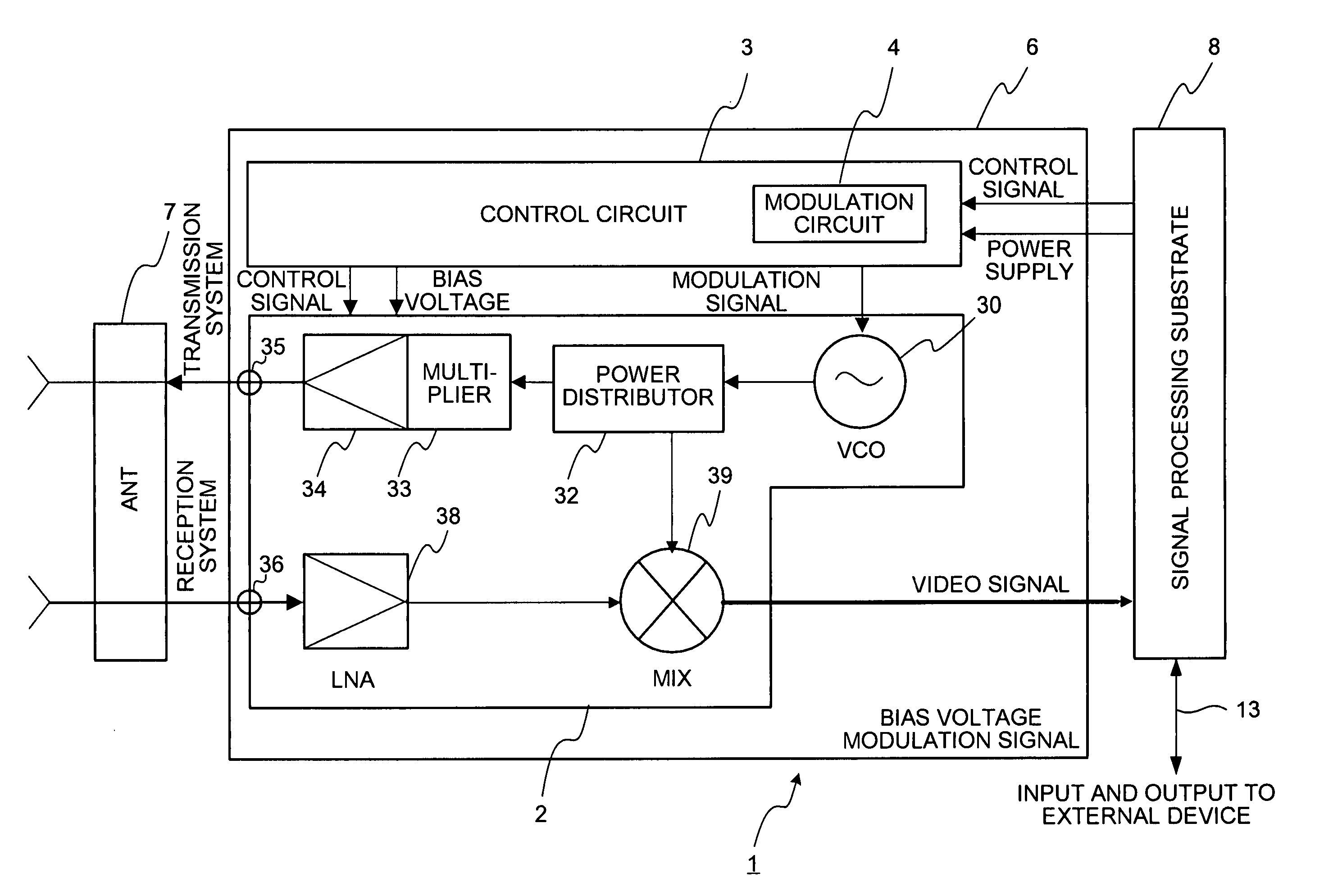
[0107]A first embodiment of the present invention is explained below with reference to FIG. 1 to FIG. 18. FIG. 1 is a functional block diagram of a radar device 1 that includes a radio device to which the present invention is applied. A functional internal configuration of the radar device 1 is explained first with reference to FIG. 1.

[0108]The radar device 1 is an FM-CW radar having a function of detecting a distance and a relative speed between with respect to a target object (such as a vehicle) in front, using electromagnetic waves of a milliwave band (for example, 76 GHz). The FM-CW radar irradiates a frequency modulated high-frequency signal (a transmission signal) to the target, detects a difference in frequency between the transmission signal and a signal reflected from the target (a reception signal), and calculates a distance and a relative speed with respect to the target.

[0109]As shown in FIG. 1, the radar device 1 includes a transmission / reception module 6, an antenna 7 ...

second embodiment

[0167]A second embodiment of the present invention is explained below with reference to FIG. 19. In the second embodiment, the slot line 83 used in the first embodiment is changed to a low-pass filter 86 including a combination of plural slot lines. FIG. 20 depicts a transmission characteristic of the low-pass filter 86. This low-pass filter 86 cuts a frequency component equal to or higher than a predetermined frequency f1 lower than the frequency f0 corresponding to the effective wavelength λg of the high-frequency signal. The low-pass filter 86 is effective when many wavelength components near the effective wavelength λg are present.

[0168]According to the second embodiment, the low-pass filter 86 is provided in the internal-layer signal line 60. Consequently, the high-frequency component coupled to the signal via 65 or the internal-layer signal line 60 can be suppressed from transmitting to the internal-layer signal line 60 in front of the low-pass filter 86. As a result, leakage ...

third embodiment

[0169]A third embodiment of the present invention is explained below with reference to FIG. 21 and FIG. 22. FIG. 21 depicts a high-frequency package 2′ according to the third embodiment. In the high-frequency package 2′, like reference numerals denote like constituent elements that achieve the same functions as the constituent elements of the high-frequency package 2 shown in FIG. 6, and a redundant explanation is omitted.

[0170]The high-frequency package 2′ shown in FIG. 21 is double-side mounted. A high-frequency semiconductor (or an electronic circuit part concerning the high-frequency semiconductor) 66 is also mounted on a rear surface of the multilayer dielectric substrate 23. The high-frequency semiconductor 66 is shielded by the carrier 22 and a back-surface cover 67.

[0171]In the high-frequency package 2′ according to the third embodiment, the sidewall ground vias 81 shown in FIG. 11 or the ground pattern 85 shown in FIG. 15 is not provided near the sidewall 55 that constitute...


PUM


Abstract

A multilayer dielectric substrate includes a first signal via, a second signal via, an internal-layer signal line, an internal-layer ground conductor, and ground vias. The first signal via is connected to a bias-and-control-signal terminal of a high-frequency semiconductor, and is arranged within a region corresponding to the electromagnetic shielding members. The second signal via is arranged outside the region, and is connected to an external terminal for a bias and control signal. The internal-layer signal line connects between the first and the second signal vias. The internal-layer ground conductor is arranged around the first and the second signal vias and the internal-layer signal line. The ground vias are arranged around the first and the second signal vias and the internal-layer signal line, on the internal-layer ground conductor. A resistance film is provided on at least one of an upper surface and a lower surface of the internal-layer signal line.

Description

TECHNICAL FIELD[0001]The present invention relates to a high-frequency package that includes a high-frequency semiconductor that operates in a high-frequency band such as a microwave band and a milliwave band, a transmission / reception module, and a radio device that include the high-frequency package. More particularly, the present invention relates to a high-frequency package that can suppress leakage of a high-frequency signal generated from the high-frequency semiconductor to outside, a transmission / reception module, and a radio device that include the high-frequency package.BACKGROUND ART[0002]Conventionally, radio device, for example, a milliwave radar mounted on a vehicle uses electromagnetic waves of a milliwave band, and detects a distance and a relative speed between the vehicle and a vehicle running in front to be applied to achieve a cruise control and a safety measure to reduce damage on a driver when a collision cannot be avoided. In many cases, such an in-vehicle milli...

Claims


Application Information

Patent Timeline
Patent Type & Authority Patents(United States)
IPC IPC(8): G01S7/28H01L23/02H01L23/12H01L23/552H01L23/66H05K1/00H05K1/02H05K1/16H05K1/18
CPCH01L23/552H05K1/167H01L23/66H01L2224/16235H01L2224/45014H01L2224/48091H01L2924/01004H01L2924/01057H01L2924/01079H01L2924/14H01L2924/1423H01L2924/15153H01L2924/1517H01L2924/15192H01L2924/16195H01L2924/19107H01L2924/3025H05K1/0219H05K1/0243H05K1/0298H05K1/183H05K2201/09536H05K2201/09618H05K2201/10371H01L2924/01019H01L2224/73265H01L2224/48227H01L2224/32225H01L24/48H01L24/45H01L2224/16225H01L2924/00014H01L2924/00012H01L2924/00H01L24/73H01L2224/05554H01L2924/10162H01L24/49H01L2224/49175H01L2924/206
Inventor MATSUO, KOICHITAMAKI, TSUTOMUSUZUKI, TAKUYA
Owner MITSUBISHI ELECTRIC CORP
Why Eureka
Try Eureka