Image display device and luminance correcting method thereof

a technology of image display and luminance correction, which is applied in the direction of instruments, computing, electric digital data processing, etc., can solve the problems of reducing the luminance of light emitting elements which accompanies the deterioration of organic light emitting materials, and the inability to display desired colors on display devices, etc., to achieve high definition display, good compatibility, and sufficient output resistance

Inactive Publication Date: 2008-02-26
SEMICON ENERGY LAB CO LTD
View PDF10 Cites 27 Cited by
  • Summary
  • Abstract
  • Description
  • Claims
  • Application Information

AI Technical Summary

Benefits of technology

[0015]It is a primary object of the invention to provide an image display device wherein the current flowing to the light emitting element is controlled by controlling the current I1 with the data signal line by making no difference between the current I1 flowing through Tr1 and the current I2 flowing through Tr2. The image display device has enough output resistance not to be influenced by a variation of characteristics of light emitting elements. The image display also keeps a constant luminance even when a characteristic is remarkably changed by a deterioration of the light emitting element and a change in temperature, and is capable of high definition display.

Problems solved by technology

On commercialization of a display device using a light emitting element, however, a problem lies in the reduction in luminance of light emitting element which accompanies the deterioration of the organic light emitting material.
Therefore, a desired color cannot be displayed on a display device.

Method used


Image

  • Image display device and luminance correcting method thereof
  • Image display device and luminance correcting method thereof
  • Image display device and luminance correcting method thereof

Examples


embodiment mode 1

[Embodiment Mode 1]

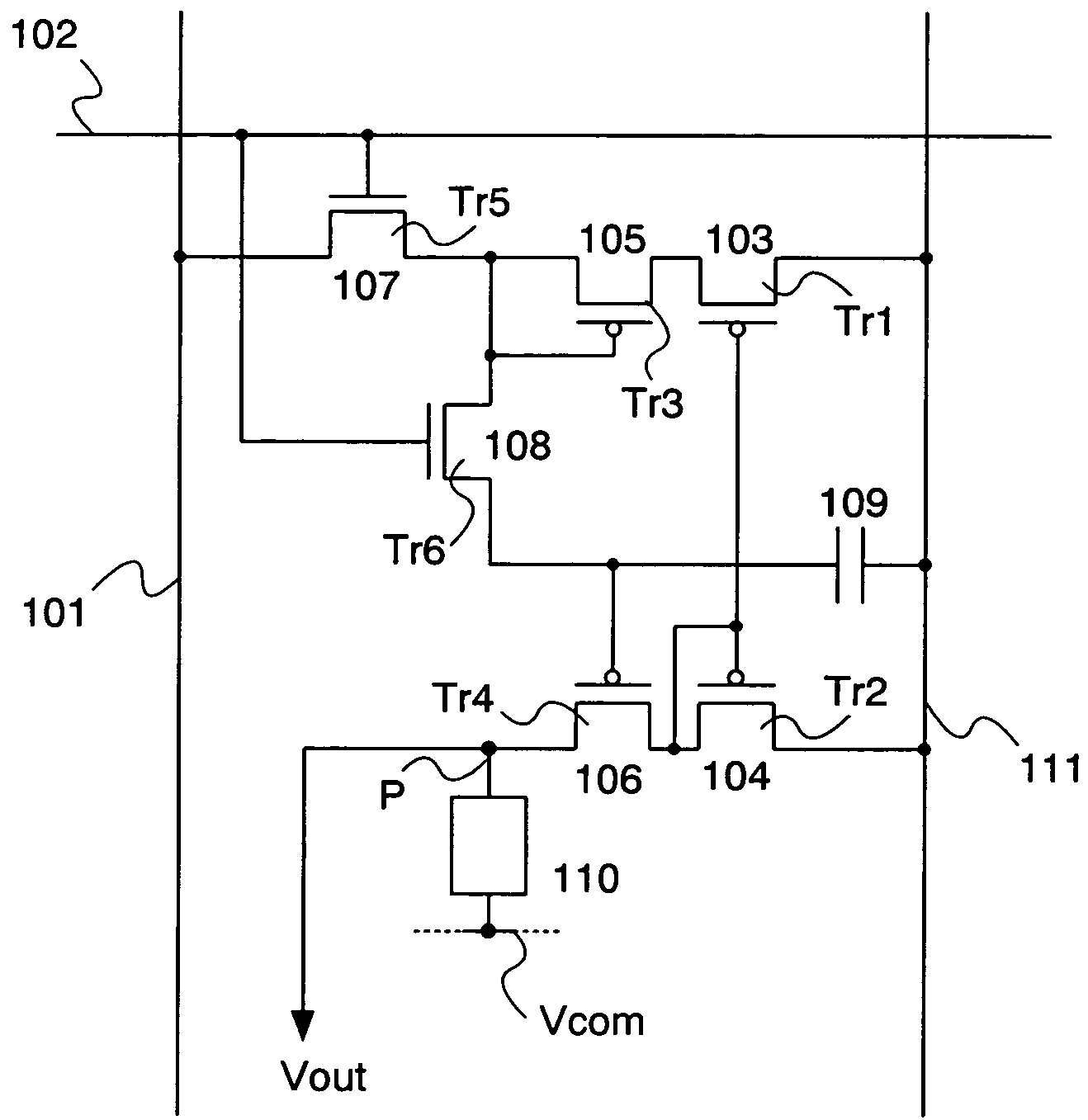
[0036]FIG. 1 shows a pixel circuit according to Embodiment Mode 1 of the invention. The pixel circuit includes a first transistor Tr1, a second transistor Tr2, a third transistor Tr3, a fourth transistor Tr4, a fifth transistor Tr5, a sixth transistor Tr6, a light emitting element 110, a power source line 111, a data signal line 101, a scanning line 102, and a capacitor 109.

[0037]Gate electrodes of the transistor Tr5 and Tr6 are both connected to the scanning line. One of a source region and a drain region of the transistor Tr5 is connected to the data signal line 101 while the other is connected to a drain region of the transistor Tr3. Further, one of a drain region and a source region of the transistor Tr6 is connected to a gate electrode and the drain region of the transistor Tr3 while the other is connected to a gate electrode of the transistor Tr4.

[0038]Source regions of the transistors Tr1 and Tr2 are both connected to the power source line. A gate electrode...

embodiment mode 2

[Embodiment Mode 2]

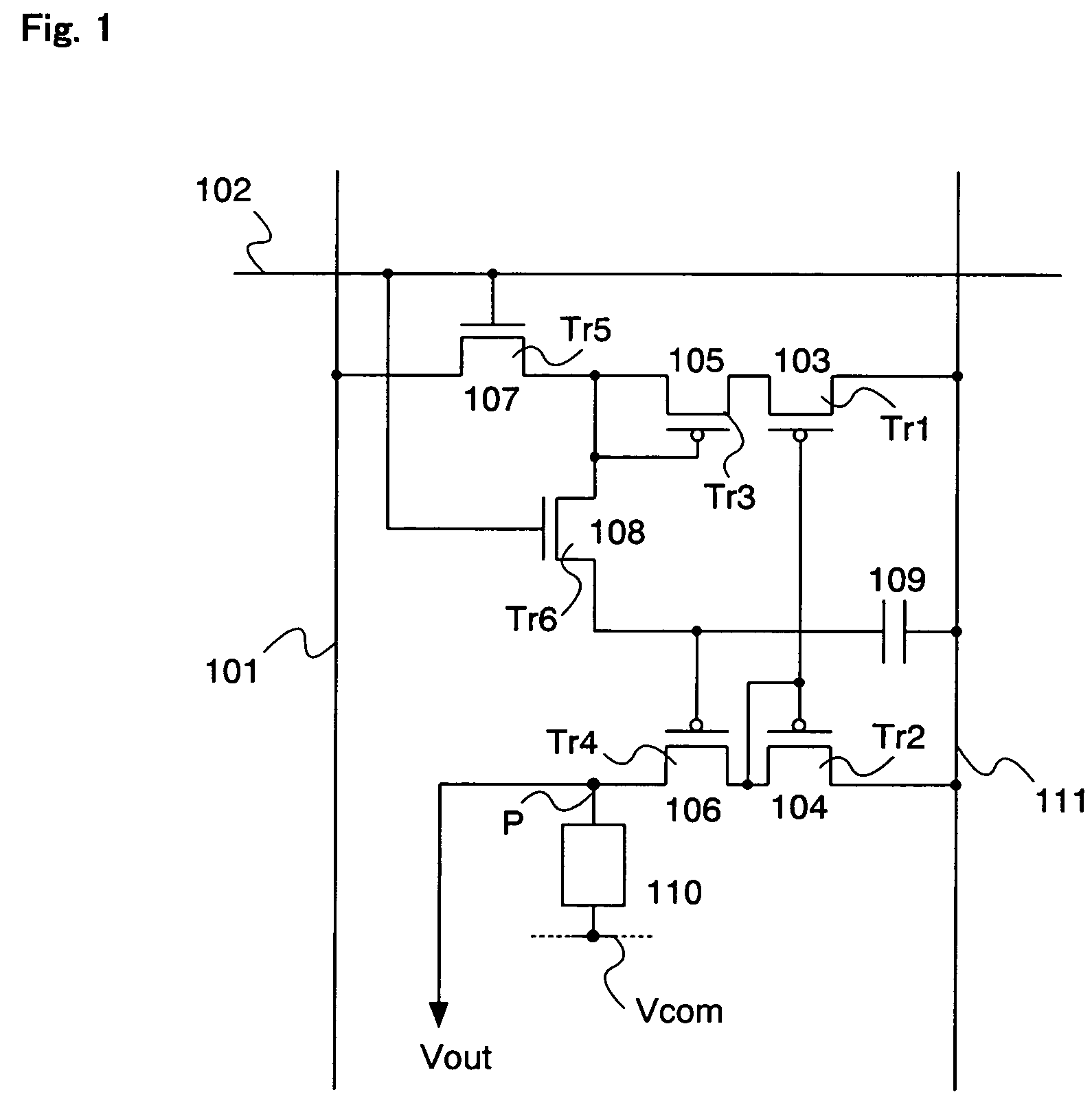
[0053]FIG. 2 shows a pixel circuit according to Embodiment Mode 2 of the invention. The pixel circuit includes a first transistor Tr1, a second transistor Tr2, a third transistor Tr3, a fourth transistor Tr4, a fifth transistor Tr5, a sixth transistor Tr6, a light emitting element 210, a power source line 211, a data signal line 201, a scanning line 202, a capacitor 209, an erasing signal line 212, and an erasing transistor 213.

[0054]The above-mentioned circuit is one in which an erasing circuit is added to the circuit of Embodiment Mode 1, and the description of the connection is made on the added circuit only. A gate electrode of the erasing transistor 213 is connected to the erasing signal line 212 and the erasing transistor 213 is provided between the power source line 211 and a gate electrode of the transistor Tr4.

[0055]A potential of the power source line 211 is kept at a constant value. Also a potential of a counter electrode is kept at a constant value dur...

embodiment mode 3

[Embodiment Mode 3]

[0059]The third Embodiment mode of the invention is explained now. FIG. 5B shows a characteristic curve of an EL element and a driving TFT. It is confirmed in FIG. 5B that an intersection point (operation point) is required to be within the saturation region of the driving TFT so as not to be influenced by the variation of the EL element. Also, in a pixel circuit of the invention, a current source is required to be set so that the transistors Tr1 to Tr4 operate in the saturation region in order to make the current value stable. However, as shown in FIG. 7, the light emitting element changes its IV characteristic according to temperature. Provided that a constant voltage is supplied, the more the temperature of the light emitting element rises, the more the driving current increases. The temperature of the light emitting element is dependent not only on the outside temperature but also on a heat generated from the panel itself, therefore a considerable care is requ...


PUM


Abstract

The purpose of the invention is providing a current-input display device which can emit light at a constant luminance and provide a high definition display. According to the invention, a current which is almost the same as a current source can be inputted by adding a transistor in a pixel circuit, the circuit has a large output resistance enough not to be influenced by a change in I-V characteristic due to a deterioration of a light emitting element, a change in temperature and the like, and a high definition display can be obtained by conducting a correction if there are any influential changes in characteristics.

Description

BACKGROUND OF THE INVENTION[0001]1. Field of the Invention[0002]The present invention relates to an image display device having a light emitting element, and more particularly, to a remedy of reduction in luminance of the light emitting element according to a deterioration of a light emitting material.[0003]2. Description of the Related Art[0004]A light emitting element represented by an electro luminescence (EL) element is high in visibility, since it emits light by itself. Therefore, the light emitting element is optimum to form in a thin shape since it does not need a backlight required for a liquid crystal display device. Further, a viewing angle of the light emitting element is not restricted. Therefore, in recent years, a display device using a light emitting element attracts attention as a display device substituted for CRT (cathode-ray tube) or LCD (liquid crystal display).[0005]On commercialization of a display device using a light emitting element, however, a problem lies ...

Claims


Application Information

Patent Timeline
Patent Type & Authority Patents(United States)
IPC IPC(8): G09G3/30G09G3/10G09G3/32G09G3/36G09G5/00G09G5/10G09G3/20
CPCG09G3/3241G09G2300/0809G09G2300/0842G09G2310/0251G09G2320/0233G09G2320/043
Inventor OSADA, TAKESHI
Owner SEMICON ENERGY LAB CO LTD
Why Eureka
Try Eureka