Autofocus methods and devices for lithography

a technology of autofocus and lithography, which is applied in the direction of photomechanical treatment, printing, instruments, etc., can solve the problems of large glancing angle af devices, inability to meet the requirements of future applications, and large overlay errors of about 10 nm, so as to reduce the amount of undesired signals, reduce signal variations, and facilitate further signal processing

Active Publication Date: 2008-03-11
NIKON CORP
View PDF15 Cites 15 Cited by
  • Summary
  • Abstract
  • Description
  • Claims
  • Application Information

AI Technical Summary

Benefits of technology

[0012]The present invention provides improved AF methods and devices for lithography. Some embodiments of the invention provide an AF system that includes one or more interferometers for measuring a distance to a target such as a wafer surface or a reticle surface. The invention includes methods and devices for calibrating the interferometer(s) according to known distances to a target. According to some embodiments of the invention, a spatial filter reduces the amount of undesired signal coming from the wafer or reticle surface. In some such embodiments, higher orders of diffracted light from the wafer or reticle multilayer surfaces are eliminated with a pinhole filter oriented to reject light that is not vertically directed. Other embodiments include a spatial filtering system that passes a selected diffraction order, e.g., the first order of diffracted light, from the target. These spatial filters reduce variations in the signal and make further signal processing easier. Employing polarized light and polarization filters also serves to reduce background signal. By including a beam expander, the interferometer beam can sample a larger or smaller area on the wafer.

Problems solved by technology

Therefore, an overlay error as large as 25 nm caused by a displacement of a reticle in the Z direction alone poses a serious problem.
This is because overlay errors of about 10 nm can be caused by other factors, e.g., alignment accuracy of a reticle and wafer, wafer stage alignment accuracy including stepping accuracy, or the distortion of the projection optical system.
Conventional glancing angle AF devices are large and may not have the accuracy required for future applications.
For application to EUV reticle height sensing, the glancing angle of such AF devices may cause interference between the AF beams and proximity illumination blinds or other structures.
Also, their accuracy may be inadequate for the <50 nm height tolerance of the EUV reticle.
Conventional glancing angle AF devices also pose problems for immersion lithography systems.
At the edge of the water, typically at the edge of the lens or supported structure near the edge of the lens, the liquid-air boundary may not be well defined and may be changing rapidly.
Temperature gradients in the water also cause problems for the AF.
Transmitting an AF / AL beam through this interface using prior art AF systems causes substantial disruption and subsequent loss of signal, and hence performance.

Method used


Image

  • Autofocus methods and devices for lithography
  • Autofocus methods and devices for lithography
  • Autofocus methods and devices for lithography

Examples


Embodiment Construction

[0043]In this application, numerous specific details are set forth in order to provide a thorough understanding of the present invention. It will be obvious, however, to one skilled in the art, that the present invention may be practiced without some or all of these specific details. In other instances, well known process steps have not been described in detail in order not to obscure the present invention.

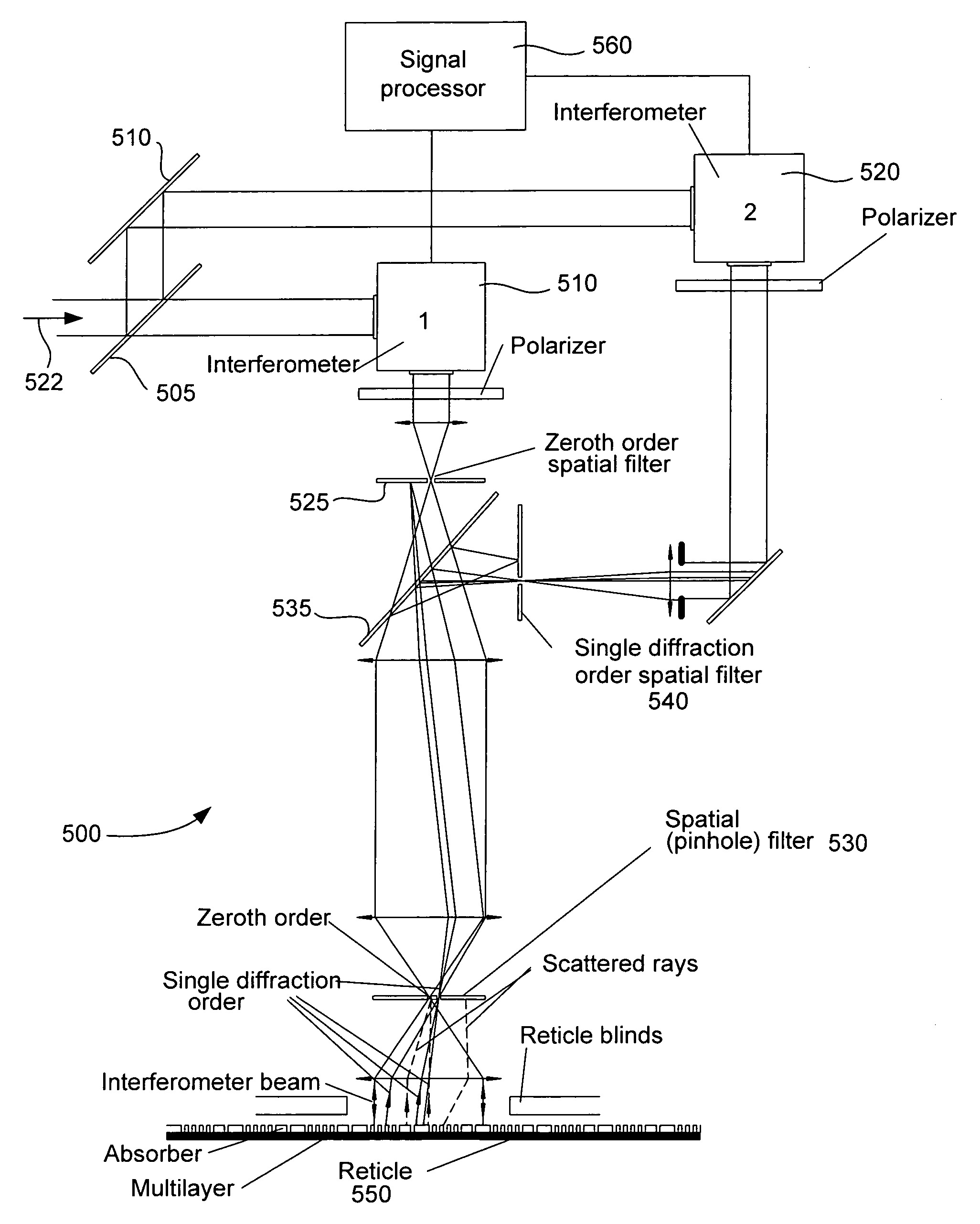
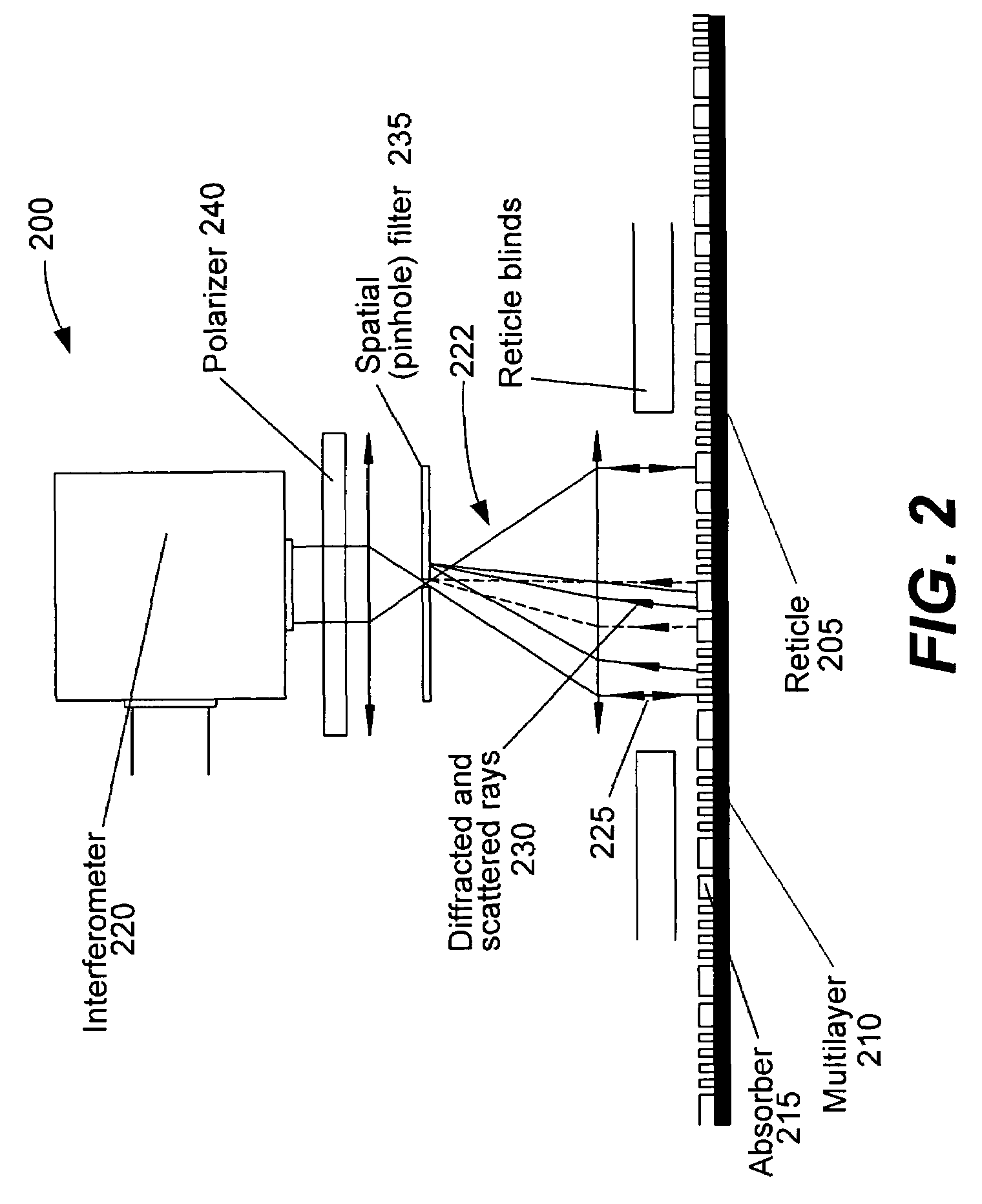
[0044]The invention includes various AF devices and methods for reducing the amount of undesired signal coming from a wafer or reticle surface. A significant fraction of light reaching the wafer or reticle surface will be diffracted by the patterned surface. First-order diffracted light and higher orders of diffracted light from such a surface will not be oriented vertically, but instead will emerge at angles to normal incidence. According to some embodiments of the invention, first-order diffracted light and higher orders of diffracted light are eliminated with a pinhole spatial ...


PUM


Abstract

Improved autofocusing (“AF”) methods and devices for lithography are provided. Some embodiments of the invention provide an AF system that includes one or more interferometers for measuring a distance to a wafer surface or a reticle surface. The invention includes methods and devices for calibrating the interferometer(s) according to known distances to a target. According to some embodiments of the invention, a spatial filter reduces the amount of undesired signal coming from the wafer or reticle surface. In some such embodiments, higher orders of diffracted light from the wafer or reticle multilayer surfaces are eliminated with a pinhole filter oriented to reject light that is not vertically directed. Other embodiments include a spatial filtering system that passes a selected diffraction order, e.g., the first order of diffracted light, from the target.

Description

BACKGROUND OF THE INVENTION[0001]This invention relates to autofocus devices and methods for use in lithography.[0002]Currently, at the sites which manufacture semiconductor devices, circuit devices are mass-produced by using reduction projection exposure devices, using the i line from mercury lamps that has a wavelength of 365 nm as an illumination light. At the same time, the introduction of exposure devices of the next generation, having minimum line widths of 0.25 μm, has begun.[0003]A scanning exposure apparatus based on the step-and-scan method is being developed. This apparatus uses an ultraviolet pulse laser beam with a wavelength of 248 nm from a KrF excimer laser source or an ultraviolet pulse laser beam with a wavelength of 193 nm from an ArF excimer laser source as an illumination light. A scanning exposure apparatus then linearly scans a mask or a reticle (to be generically referred to as a “reticle” hereinafter) on which a circuit pattern is drawn and a wafer serving a...

Claims


Application Information

Patent Timeline
Patent Type & Authority Patents(United States)
IPC IPC(8): G03B27/52G03B27/54
CPCG03F9/7026G03F9/7049
Inventor SOGARD, MICHAEL
Owner NIKON CORP
Why Eureka
Try Eureka