Circuit and method for adaptive incremental step-pulse programming in a flash memory device

a flash memory device and incremental step technology, applied in the field of integrated circuit memory devices, can solve the problems of loss of operating speed, excessive increase of program voltage step, long overall programming time, etc., and achieve the effect of improving the threshold voltage distribution, reducing the magnitude of programming voltage step, and increasing the duration of verification operations

a flash memory device and incremental step technology, applied in the field of integrated circuit memory devices, can solve the problems of loss of operating speed, excessive increase of program voltage step, long overall programming time, etc., and achieve the effect of improving the threshold voltage distribution, reducing the magnitude of programming voltage step, and increasing the duration of verification operations

US7349263B2Active Publication Date: 2008-03-25SAMSUNG ELECTRONICS CO LTD

Image

  • Circuit and method for adaptive incremental step-pulse programming in a flash memory device
  • Circuit and method for adaptive incremental step-pulse programming in a flash memory device
  • Circuit and method for adaptive incremental step-pulse programming in a flash memory device

Examples


Embodiment Construction

[0020]The present invention now will be described more fully herein with reference to the accompanying drawings, in which preferred embodiments of the invention are shown. This invention may, however, be embodied in many different forms and should not be construed as being limited to the embodiments set forth herein; rather, these embodiments are provided so that this disclosure will be thorough and complete, and will fully convey the scope of the invention to those skilled in the art. Like reference numerals refer to like elements throughout and signal lines and signals thereon may be referred to by the same reference characters.

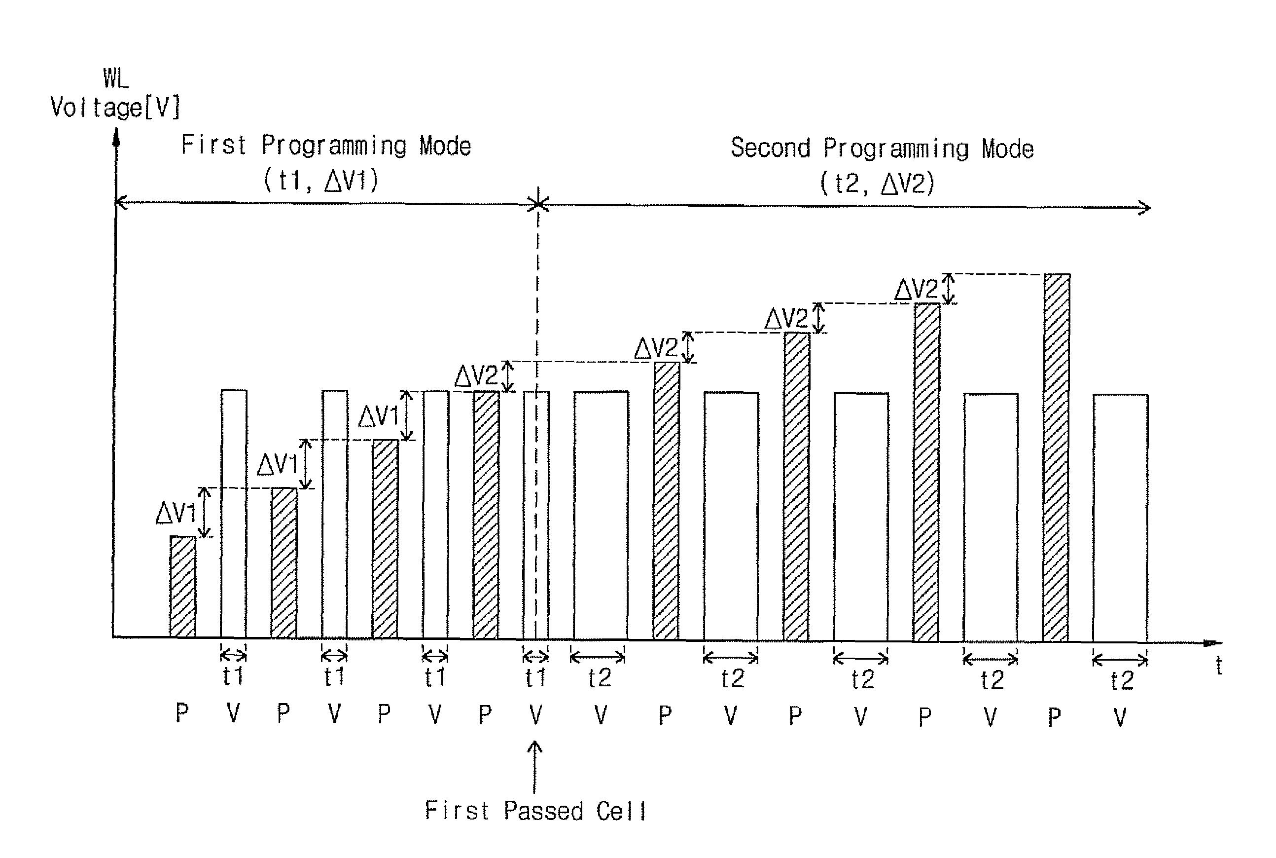
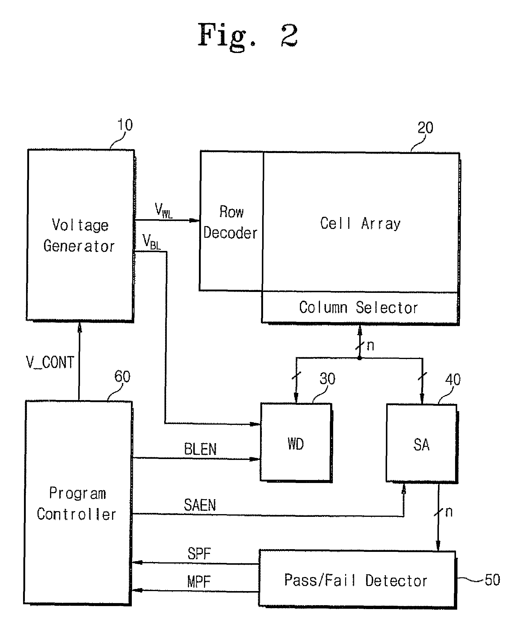
[0021]FIG. 2 is a block diagram illustrating a functional structure for a programming operation in a flash memory according to an embodiment of the present invention. The flash memory device includes a memory cell array 20 coupled to a row decoder and a column selector, a voltage generator 10 supplying a program voltage Vpgm and a verifying voltage Vveri to...


PUM


Abstract

Nonvolatile memory devices support programming and verify operations that improve threshold-voltage distribution within programmed memory cells. This improvement is achieved by reducing a magnitude of the programming voltage steps and increasing a duration of the verify operations once at least one of the plurality of memory cells undergoing programming has been verified as a “passed” memory cell. The nonvolatile memory device includes an array of nonvolatile memory cells and a control circuit, which is electrically coupled to the array of nonvolatile memory cells. The control circuit is configured to perform a plurality of memory programming operations (P) by driving a selected word line in the array with a first stair step sequence of program voltages having first step height (e.g., ΔV1) and then, in response to verifying that at least one of the memory cells coupled to the selected word line is a passed memory cell, driving the selected word line with a second stair step sequence of program voltages having a second step height (e.g., ΔV2) lower than the first step height.

Description

REFERENCE TO PRIORITY RELATED APPLICATION[0001]This patent application claims priority under 35 U.S.C. § 119 to Korean Patent Application 2005-55906 filed on Jun. 27, 2005, the entire contents of which are hereby incorporated herein by reference.FIELD OF THE INVENTION[0002]The present invention relates to integrated circuit memory devices and, more particularly, to flash memory devices and methods of operating flash memory devicesBACKGROUND OF THE INVENTION[0003]Flash memory devices are a type of nonvolatile semiconductor memory device. Flash memory devices are regarded as being highly adaptable to large storage capacities and high-frequency operation in applications requiring large-capacity storage devices and coded memories for mobile apparatuses. Flash memory devices are generally classified into BAND and NOR types by the logical pattern of the cell array. The memory cell array of the NOR-type flash memory device is structured such that a plurality of memory cells are arranged as...

Claims


Application Information

Patent Timeline
25 Mar 2008
Publication
US7349263B2
IPC
G11C11/34
CPC
G11C16/12; G11C16/3454; G11C16/3459
Inventors
KIM, SOO-HAN; JEONG, JAE-YONG