

Optical waveguide device, manufacturing method thereof, optical information processing apparatus, and electronic equipment
a technology of optical waveguides and manufacturing methods, applied in the direction of optical waveguide light guides, instruments, optics, etc., can solve the problems of rc signal delay, data exchange amount required between, occurrence of various high-frequency problems, etc., and achieve the effect of improving yield and easy and precise performan
- Summary
- Abstract
- Description
- Claims
- Application Information
AI Technical Summary
Benefits of technology
Problems solved by technology
Method used
Image

Examples
first preferred embodiment
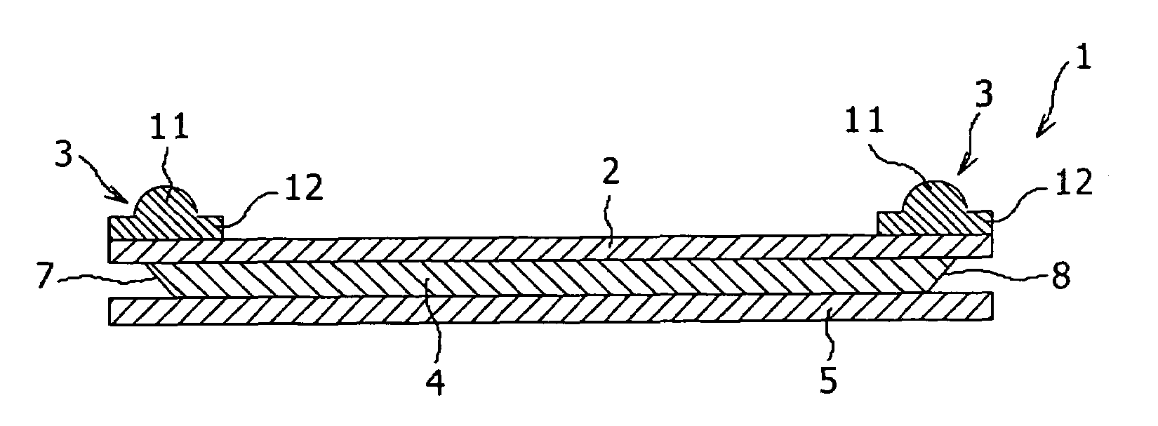
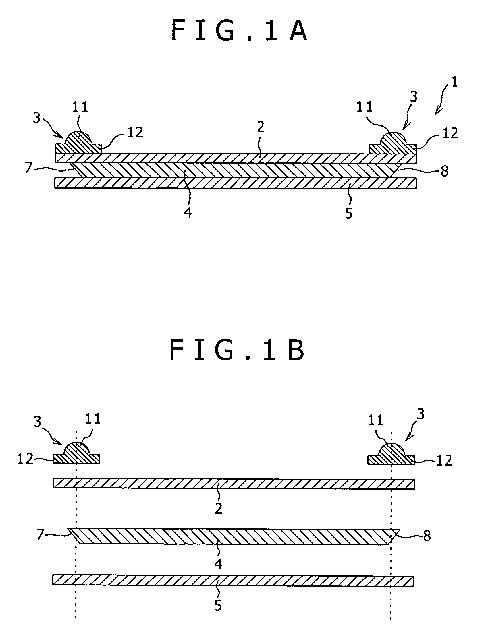
[0075]FIG. 1A is a schematic sectional view of an optical waveguide device 1 according to the present invention, and FIG. 1B is an exploded view of FIG. 1A.
[0076]As shown in FIGS. 1A and 1B, the optical waveguide device 1 has a laminated structure composed of a first cladding 2, a second cladding 5 independent of the first cladding 2, and a core 4 sandwiched between the first and second claddings 2 and 5, wherein light is guided in the core 4. The core 4 serves to guide an incident optical signal, and the claddings 2 and 5 serve to confine the optical signal in the core 4. The core 4 is formed of a material having a high refractive index, and the claddings 2 and 5 are formed of a material having a refractive index lower than that of the core 4.
[0077]The cladding 2 is formed from a flexible sheet, and a pair of light collimating or a focusing section 3 are bonded to the upper surface of the cladding 2 at its opposite ends corresponding to light incident and emergent portions 7 and 8 ...
second preferred embodiment
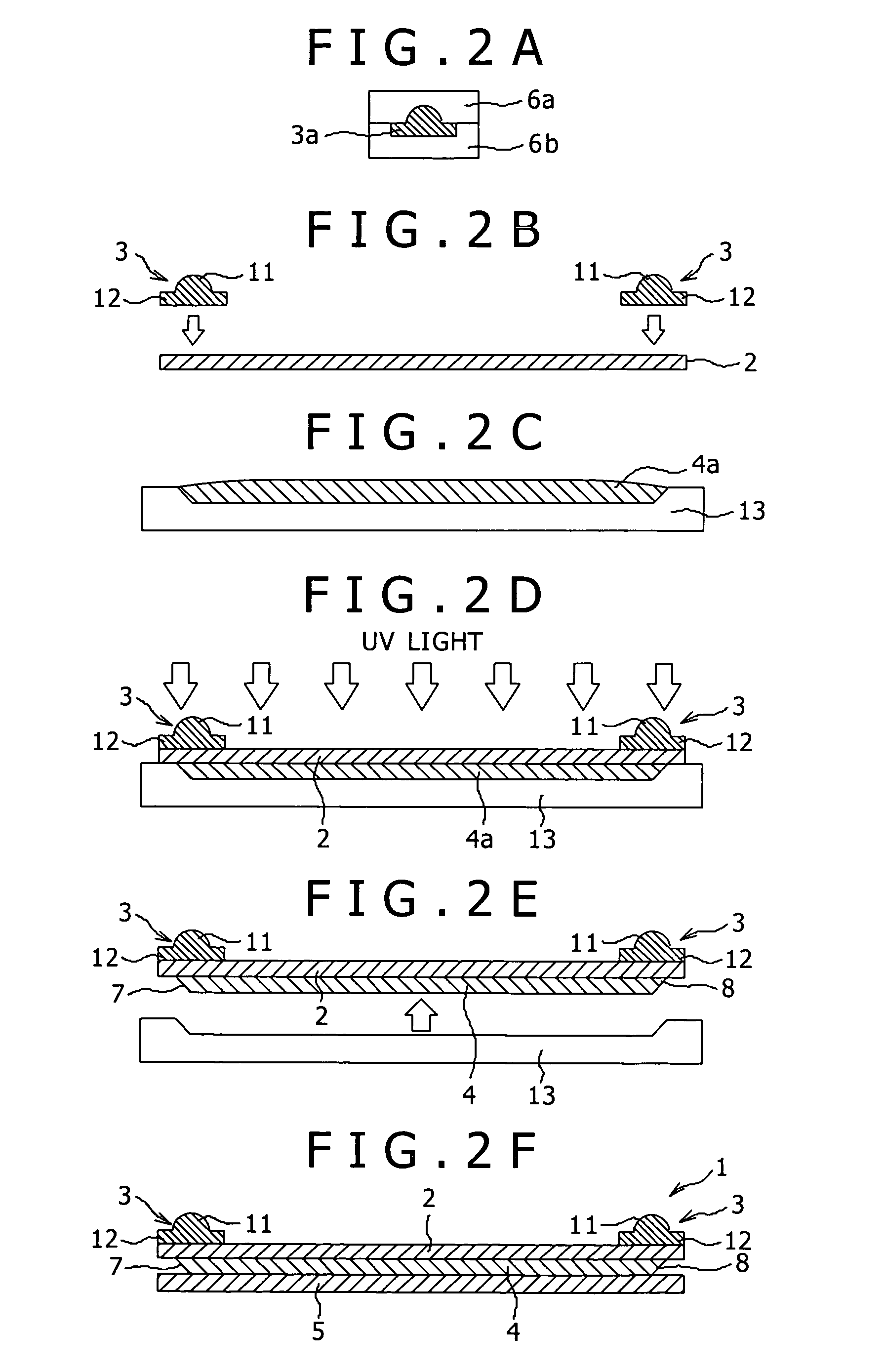
[0094]FIGS. 3A to 3E are schematic sectional views showing another manufacturing method for the optical waveguide device 1.
[0095]As shown in FIG. 3A, a core material 4a is filled into a mold 13. As shown in FIG. 3B, the first cladding 2 formed from a flexible sheet is attached to the upper surface of the mold 13 with the core material 4a interposed between the cladding 2 and the mold 13, and UV light is next applied to thereby cure the core material 4a. As shown in FIG. 3C, the mold 13 is removed to obtain a laminated structure composed of the cladding 2 and the core 4.
[0096]As shown in FIG. 3D, the pair of light collimating or a focusing section 3 (each formed as an integral member composed of the lens portion 11 and the lens supporting portion 12) previously fabricated by injection molding as similar to the step of FIG. 2A are bonded to the upper surface of the cladding 2 opposite to the lower surface thereof where the core 4 is bonded, at the opposite ends corresponding to the li...
third preferred embodiment
[0099]FIGS. 4A to 4C show an optical information processing apparatus 14 according to the present invention which includes an optical waveguide device 1 according to the present invention, a plurality of light emitting devices (e.g., lasers) 9 for respectively launching light into a plurality of cores 4 of the optical waveguide device 1, and a plurality of light receiving devices (e.g., photodetectors) 10 for respectively receiving emergent light from the plural cores 4. More specifically, FIG. 4A is a schematic sectional view of the optical information processing apparatus 14, FIG. 4B is a bottom plan view of the optical waveguide device 1 shown in FIG. 4A with the second cladding 5 removed, and FIG. 4C is a top plan view of the optical waveguide device 1 shown in FIG. 4A.
[0100]As shown in FIG. 4B, the plural cores 4 are arranged in parallel with a given pitch on the cladding 2, and each core 4 has a pair of light incident and emergent portions 7 and 8 each formed as a 45° mirror s...
PUM
 Abstract
Description
Claims
Application Information