Ball Grid Array package having integrated antenna pad

Inactive Publication Date: 2008-05-06
CYPRESS SEMICON CORP
View PDF17 Cites 24 Cited by
  • Summary
  • Abstract
  • Description
  • Claims
  • Application Information

AI Technical Summary

Benefits of technology

[0007]According embodiments of the invention, a BGA package including an integrated antenna i

Problems solved by technology

This electrical path can pick up inductance, and negatively effect the performance of the device.
Excess inductance limit

Method used


Image

  • Ball Grid Array package having integrated antenna pad
  • Ball Grid Array package having integrated antenna pad
  • Ball Grid Array package having integrated antenna pad

Examples


Example

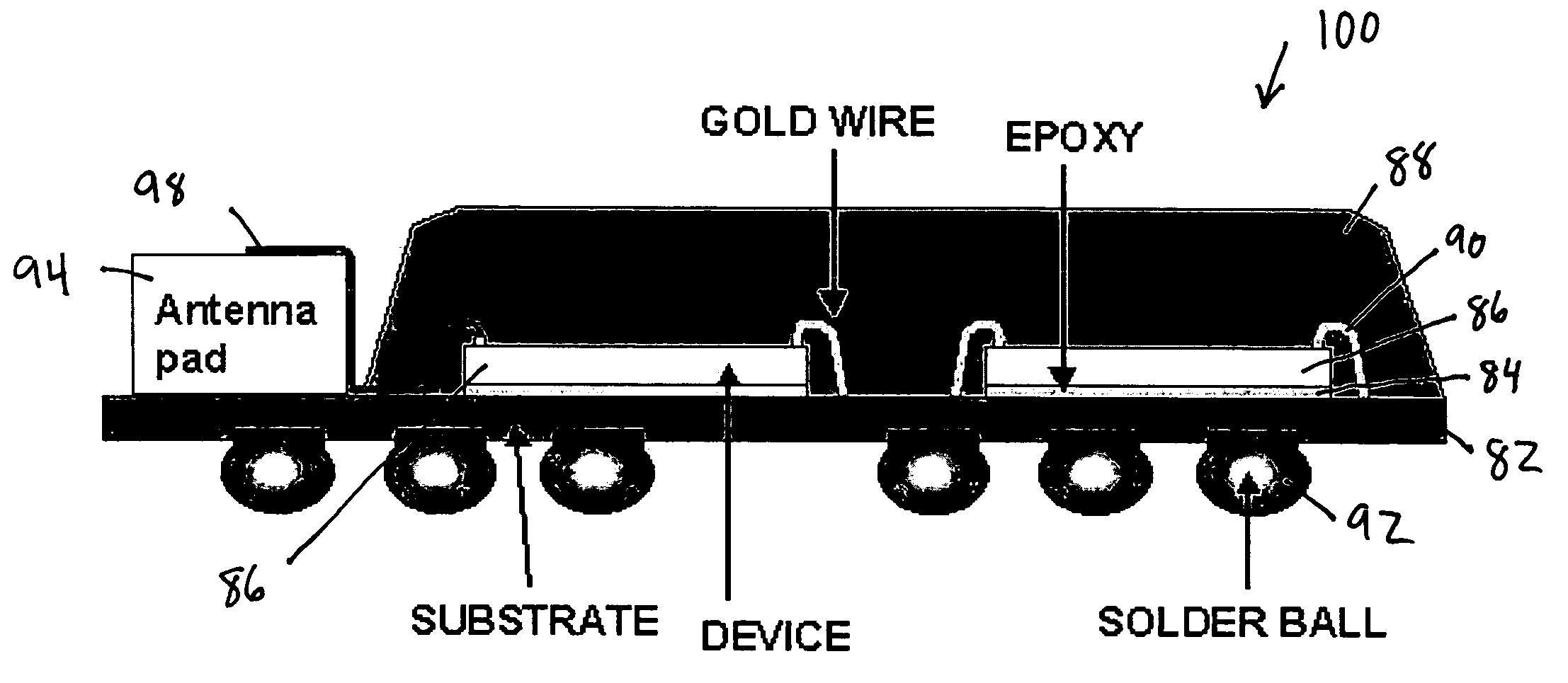
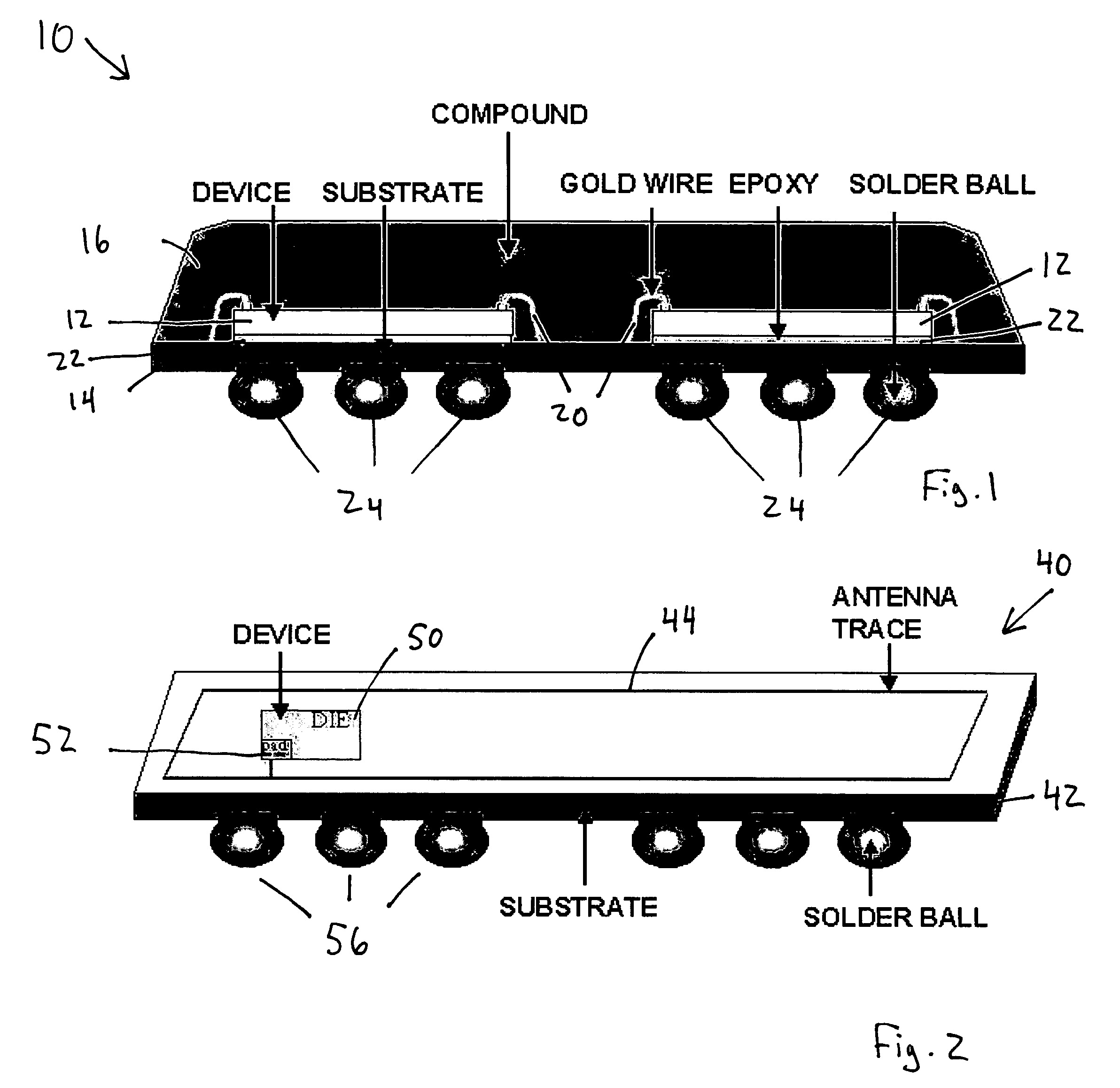
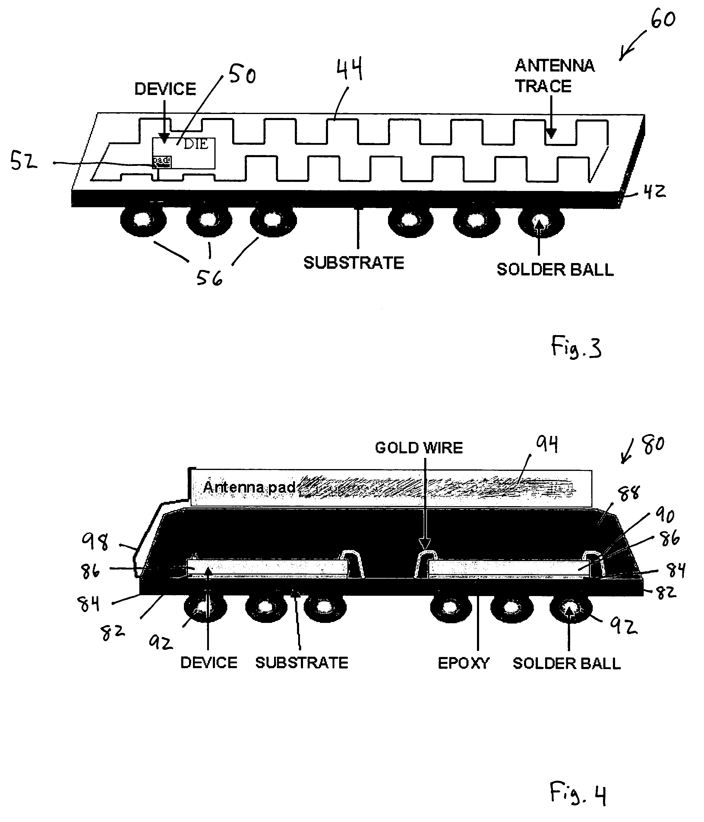
[0014]Embodiments of the invention are directed toward a package, such as a BGA package that includes a connection for an antenna that is also connected to the package. The antenna may be incorporated directly on a BGA substrate. In these ways, less inductance appears in the antenna path and antenna circuits are more efficient than is otherwise presently possible.

[0015]Present wireless communication devices include a radio incorporated on an integrated circuit chip. Antennas are used to transmit and receive the wireless signals. Antennas are implemented as conductive lengths of material having a variety of shapes to optimize reception and transmission properties. As a general rule, antenna lengths range from a half wavelength to under one tenth wavelength of the transmitted or received signal, depending upon the antenna configuration and the level of acceptable performance. Space must be allocated to accommodate the antenna and allow for adequate transmission and reception.

[0016]An ...


PUM


Abstract

An apparatus for an improved Ball Grid Array (BGA) package includes a semiconductor device having a radio frequency (RF) input or output, an antenna pad, and a BGA package structured to house the semiconductor device and the antenna pad. The antenna pad may be coupled to the radio frequency (RF) input or output, and the antenna pad is structured to reduce the inductance of the BGA package. The antenna pad may include a pad disposed above the semiconductor device, a pad disposed to the side of the semiconductor device, or an antenna chip. An antenna may be coupled to the antenna pad. The antenna may include a trace antenna, a staggered antenna, or a helical antenna.

Description

CROSS REFERENCE TO RELATED APPLICATIONS[0001]This application is a Continuation In Part of and claims priority from U.S. patent application Ser. No. 10 / 147,827, filed on 17 May 2002, now U.S. Pat. No. 6,914,566, which in turn claims priority from U.S. Provisional Application No. 60 / 291,721, filed on 17 May 2001. U.S. Pat. No. 6,914,566 and U.S. Provisional Application No. 60 / 291,721 are incorporated by reference.TECHNICAL FIELD[0002]This disclosure relates generally to packaged semiconductor devices, and, in particular to Ball Grid Array (BGA) packages for wireless devices.BACKGROUND OF THE INVENTION[0003]Allowing devices to connect to computers through a wireless communication path and wirelessly networking groups of computers is one of the fastest growing segments of the PC industry. Present and emerging standing technologies in this field include IEEE 802.11 (versions a, b and g) also known as ‘WiFi’ available from (# sign used to prevent automatic hyperlinks) http:#standards.iee...

Claims


Application Information

Patent Timeline
IPC IPC(8): H01Q1/24H01Q9/06H01Q9/26H01Q9/28H05K1/02H05K3/34
CPCH01Q1/242H01Q1/52H01Q9/26H01Q9/285H01L23/66H01Q9/065H01Q1/2283H01L24/81H01L21/56H05K1/0243H05K3/3436H01L23/3128H01L24/29H01L24/32H01L24/45H01L24/48H01L24/73H01L25/0655H01L2223/6677H01L2224/2919H01L2224/32225H01L2224/45144H01L2224/48227H01L2224/73265H01L2924/01013H01L2924/01014H01L2924/01028H01L2924/1421H01L2924/15311H01L2924/14H01L2924/30107H01L2924/3011H01L2924/00012H01L2924/00H01L2924/15787H01L2924/181
Inventor BEARD, PAUL
Owner CYPRESS SEMICON CORP
Why Eureka
Try Eureka