Active matrix type display device having antistatic lines used as repair lines

a display device and anti-static technology, applied in semiconductor devices, identification means, instruments, etc., can solve the problems of abnormal display, high-reliable repair becomes impossible in the manufacturing step of the module (md), and increase the signal delay, so as to reduce the raw manufacturing cost, high reliability, and compact mounting

Active Publication Date: 2008-05-13
JAPAN DISPLAY INC +1
View PDF5 Cites 26 Cited by
  • Summary
  • Abstract
  • Description
  • Claims
  • Application Information

AI Technical Summary

Benefits of technology

[0016]According to the present invention, it is possible to obtain following advantageous effects.[0017](1) Since the repair lines and signal-line lead lines do not cross each other, it is possible to provide the highly reliable repair in respective steps constituted of the TFT manufacturing step, the panel manufacturing step and the module manufacturing step.[0018](2) Since the short-circuiting lines remain on the substrate and hence, defects which may be caused by electric stress such as electrostatic charge or mechanical stress such as cutting can be reduced.[0019](3) There exist hardly portions of the substrate to be removed and hence, recycling is unnecessary. In case of a large-sized panel which can only take one panel from each substrate, cutting of the substrate can be completely eliminated.[0020](4) With the adoption of the COG mounting method, it is possible to reduce a raw manufacturing cost and compact mounting.
[0017](1) Since the repair lines and signal-line lead lines do not cross each other, it is possible to provide the highly reliable repair in respective steps constituted of the TFT manufacturing step, the panel manufacturing step and the module manufacturing step.
[0018](2) Since the short-circuiting lines remain on the substrate and hence, defects which may be caused by electric stress such as electrostatic charge or mechanical stress such as cutting can be reduced.
[0019](3) There exist hardly portions of the substrate to be removed and hence, recycling is unnecessary. In case of a large-sized panel which can only take one panel from each substrate, cutting of the substrate can be completely eliminated.
[0020](4) With the adoption of the COG mounting method, it is possible to reduce a raw manufacturing cost and compact mounting.
[0021]An active matrix type display device includes inter-pad short-circuiting lines which are connected with signal lines for supplying signals to TFTs, terminal portions which transmit signals from an IC chip to the signal lines, and short-circuiting lines which are provided outside the terminal portions and inside an end surface of the substrate and are connected with the plurality of inter-pad short-circuiting lines, wherein cut regions for the inter-pad short-circuiting lines are arranged outside the terminal portions and inside the short-circuiting lines.

Problems solved by technology

As described above, the conventional display device which is constituted of the display panel on which the pixels having TFTs are arranged in a matrix array has following drawbacks.(1) The display panel includes many portions where repair lines cross input lines to the TFTs and hence, the signal delay is increased due to the influence of crossing capacitances thus giving rise to the abnormal display.
Further, there may arise a situation in which the highly reliable repair becomes impossible in the module (MD) manufacturing step.(2) Since the outer periphery is cut and removed in the course of the panel manufacture, the display panel exhibits the structure which is fragile to the electrostatic stress in the succeeding step.
Further, such an operation pushes up a manufacturing cost and also requires a considerable time.(4) Since portions of the substrate to be removed are relatively large, the treatment for discarding or recycling the waste substrate becomes necessary.

Method used


Image

  • Active matrix type display device having antistatic lines used as repair lines
  • Active matrix type display device having antistatic lines used as repair lines
  • Active matrix type display device having antistatic lines used as repair lines

Examples


embodiment 1

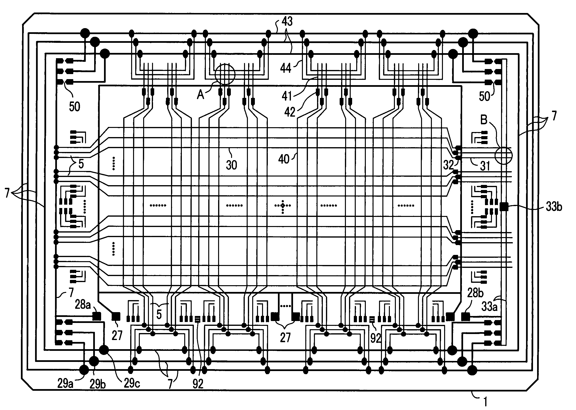
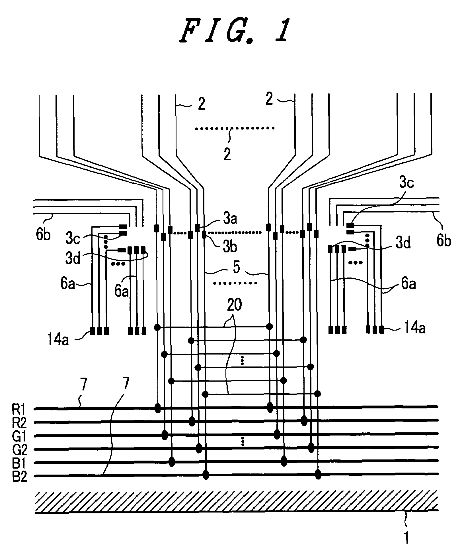
[0136]FIG. 1 is a plan view of an essential part of a transparent insulation substrate which constitutes a liquid crystal panel of an active matrix type liquid crystal display device of the present invention. FIG. 27 is a plan view of a terminal forming surface of an IC chip. Numeral 1 indicates the transparent insulation substrate (preferably a glass substrate and also simply referred to as an insulation substrate, further, also referred to as a thin film transistor substrate, a TFT substrate) which constitutes one substrate. Numeral 2 indicates input lines which are provided for thin film transistors (TFT), numerals 3a, 3b indicate connection pads to which output terminals 10a, 10b of the IC chip are connected, numerals 3c, 3d indicate input pads to which input terminals 11a, 11b of the IC chip are connected, numeral 5 indicates inter-pad short-circuiting lines, numeral 6a indicates input lines which are provided for a semiconductor integrated circuit (an IC chip) of a drive circu...

embodiment 2

[0165]The embodiment 2 of the present invention is explained in conjunction with FIG. 17 to FIG. 19. FIG. 17 is a plan view of an essential part similar to FIG. 1 for explaining the embodiment 2 of the present invention. In FIG. 17, numeral 200 indicates an end surface of a substrate after cutting the substrate and numeral 210 indicates connection terminal portions with FPC lines, wherein numerals which are equal to the numerals in FIG. 1 indicate identical functional parts. FIG. 18 is a plan view of an essential part similar to FIG. 2 for explaining the embodiment 2 of the present invention. In FIG. 18, numeral 14a indicates connection portions. Further, in FIG. 18, numeral 220 indicates an FPC, numeral 221 indicates lines in the inside of the FPC, numeral 230 indicates a printed circuit board, and numeral 231 indicates lines inside the printed circuit board. FIG. 19 is a plan view of an essential part similar to FIG. 13 for explaining an embodiment 2 of the present invention. In F...

embodiment 3

[0169]The embodiment 3 of the present invention is explained in conjunction with FIG. 20 and FIG. 21. FIG. 20 is a plan view of an essential part similar to FIG. 1 for explaining the embodiment 3 of the present invention. In FIG. 20, numeral 300 indicates a tape carrier package (TCP) and numeral 310 indicates connection terminal portions with FPC lines, wherein numerals which are equal to the numerals in FIG. 1 and FIG. 17 indicate identical functional parts. FIG. 21 is a plan view of an essential part similar to FIG. 13 for explaining the embodiment 3 of the present invention. In FIG. 21, numeral 26 indicates portions where the lines on different layers are electrically connected with each other using laser beams.

[0170]For shortening the laser cut time, in this embodiment, the connection terminal portions provided for connection with the TCP are arranged in a staggered manner so that a total end-to-end width of a plurality of inter-pad short-circuiting lines is not so elongated (FI...


PUM

PropertyMeasurementUnit
connection resistanceaaaaaaaaaa
sizeaaaaaaaaaa
drain-signal-line resistance valueaaaaaaaaaa

Abstract

An active matrix type display device includes inter-pad short-circuiting lines which are connected with signal lines, terminal portions which transmit signals from an IC chip to the signal lines, and a plurality of short-circuiting lines which are arranged outside the terminal portions and inside an end surface of a substrate and are connected with a plurality of inter-pad short-circuiting lines, wherein cut regions of the inter-pad short-circuiting lines are arranged outside the terminal portions and inside the short-circuiting lines. Since repair lines and signal-line lead line do not cross each other, it is possible to perform the highly reliable repair in respective manufacturing steps.

Description

BACKGROUND OF THE INVENTION[0001]1. Field of the Invention[0002]The present invention relates to an active matrix type display device, and more particularly to an active matrix type display device and a manufacturing method thereof in which, in forming pixels having thin film transistors (TFT) in a matrix array on an insulation substrate which is constituted of a bendable substrate such as a substrate which forms an insulation film on a glass substrate, a plastic sheet (a PES (Polyethersulfone) film or the like) or a steel foil, the display device exhibits the sufficient resistance against electrostatic stress, enables sufficient repair with high reliability using repair lines even when a signal line is disconnected, and realizes light-weighted and compact mounting in combination with chip-on-glass (COG) mounting.[0003]2. Description of the Related Art[0004]Hereinafter, as a display panel which constitutes an active matrix type display device, the explanation is made using a liquid ...

Claims


Application Information

Patent Timeline
Patent Type & Authority Patents(United States)
IPC IPC(8): G02F1/1333G02F1/1368G09F9/30G02F1/1345
CPCG02F1/136204G02F1/136259H01L27/124G02F1/13452H01L2224/05553H01L27/0296G02F2001/136272G02F1/136272
Inventor MATSUMOTO, SHINZOWATANABE, KUNIHIKO
Owner JAPAN DISPLAY INC
Why Eureka
Try Eureka