Optical substrate, manufacturing method thereof, planar lighting device and electrooptical device

a technology of electrooptical devices and optical substrates, which is applied in the direction of lighting and heating apparatus, instruments, mechanical equipment, etc., can solve the problems of reducing the productivity of backlights, increasing the number of steps in the process, and affecting so as to prevent the productivity from being lowered, prevent the optical function of microlens from being damaged, and prevent the effect of deteriorating the productivity of optical substrates

Inactive Publication Date: 2008-07-01
SEIKO EPSON CORP
View PDF8 Cites 12 Cited by
  • Summary
  • Abstract
  • Description
  • Claims
  • Application Information

AI Technical Summary

Benefits of technology

[0010]An advantage of the present invention is to provide an optical substrate on which a microlens and a reference area are provided in order to prevent the productivity from being lowered. The microlens has a light diffusing property and a predetermined alignment orientation can be read from the reference area. Other advantages of the invention are to provide a manufacturing method thereof, a planar lighting device equipped with the optical substrate, and an electrooptical device.
[0011]An optical substrate according to a first aspect of the invention includes an exit face through which a light entered from an incident face is emitted, a lens forming region provided on the exit face and in which a plurality of microlenses formed, the microlenses diffusing and emitting the light entered through the exit face, and a non-lens forming region provided in an area other than the lens forming region on the exit face and surrounded by the microlenses. The non-lens forming region being used to identify a predetermined direction of the substrate.
[0012]According to the first aspect of the invention, the light entered through the exit face can be diffused and emitted by the lens forming region in which the microlens are formed. A predetermined direction of the optical substrate can be identified with the non-lens forming region which is the area surrounded by the microlenses.
[0013]In other words, the non-lens forming region surrounded by the microlenses can serve as an alignment mark on the substrate. Furthermore, it is possible to make a non-forming region in the manufacturing process of the microlens. Consequently, it is possible to identify a certain direction of the substrate (for example, a placing direction and a transfer direction of the substrate, an alignment direction of the lens, a processing direction of the substrate and the like) without deteriorating the productivity of the optical substrate having the microlens.
[0014]In this case, the non-lens forming region may be provided in a peripheral area of the exit face.
[0015]In this way, the microlenses can be formed in substantially the whole area of the exit face because the non-lens forming region is provided in the peripheral area of the exit face. Accordingly, it is possible to prevent the optical function of the microlens from being lost.

Problems solved by technology

This could be a problem because it reduces the productivity of the backlight.
However, where it is attempted to form the alignment mark and the like on the light guide plate having the microlens, the microlens could be damaged during the formation process of the alignment mark.
In addition, the cost and the number of steps in the process would be increased in order to form the alignment mark.
This could reduce the productivity of the light guide plate and the productivity of the backlight could not be improved.

Method used


Image

  • Optical substrate, manufacturing method thereof, planar lighting device and electrooptical device
  • Optical substrate, manufacturing method thereof, planar lighting device and electrooptical device
  • Optical substrate, manufacturing method thereof, planar lighting device and electrooptical device

Examples


Embodiment Construction

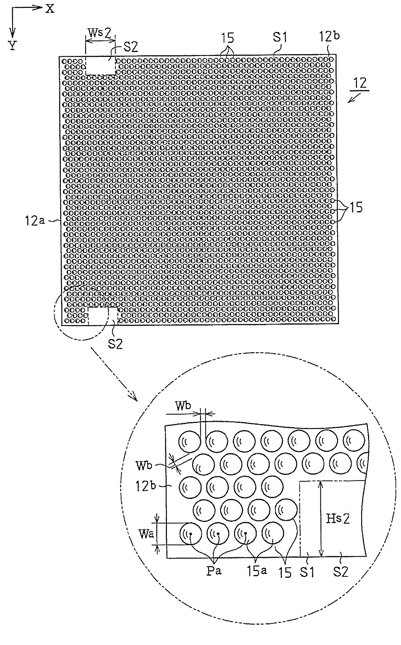
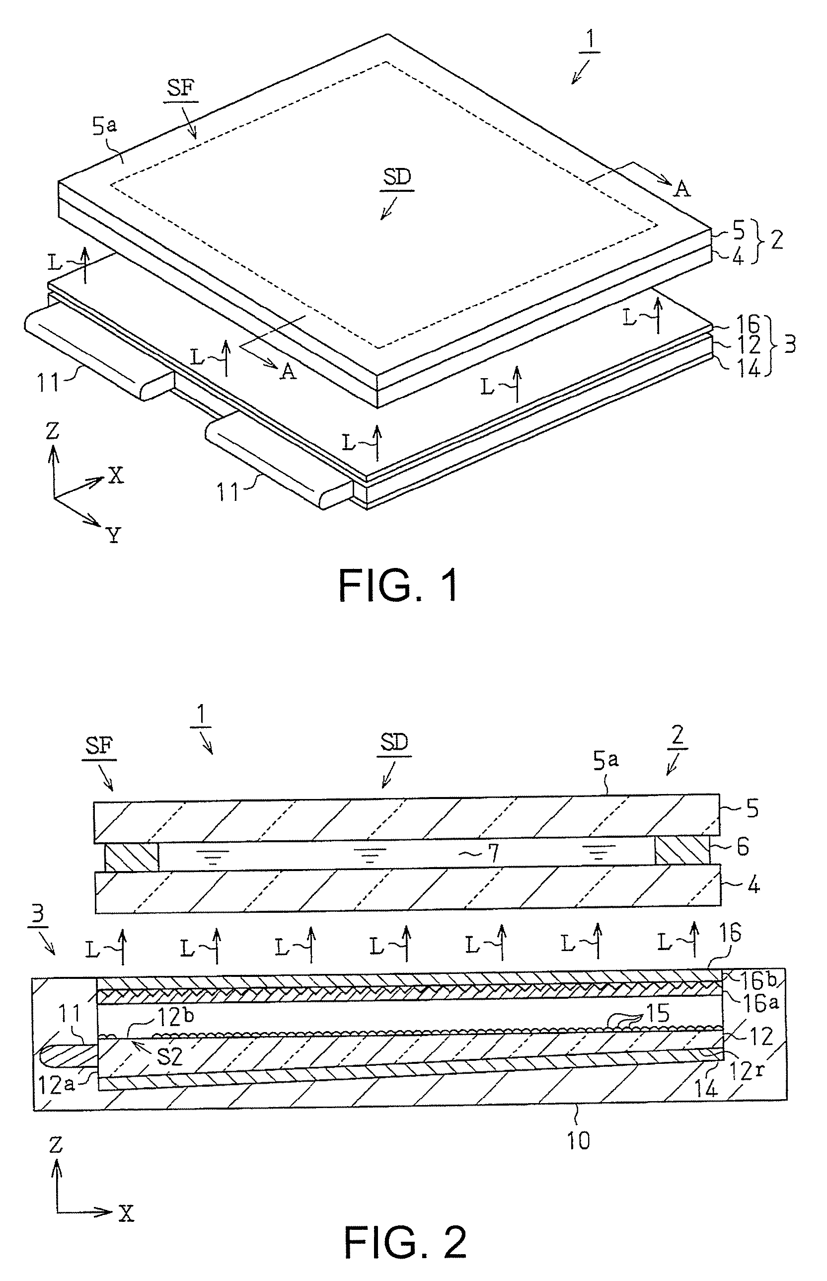
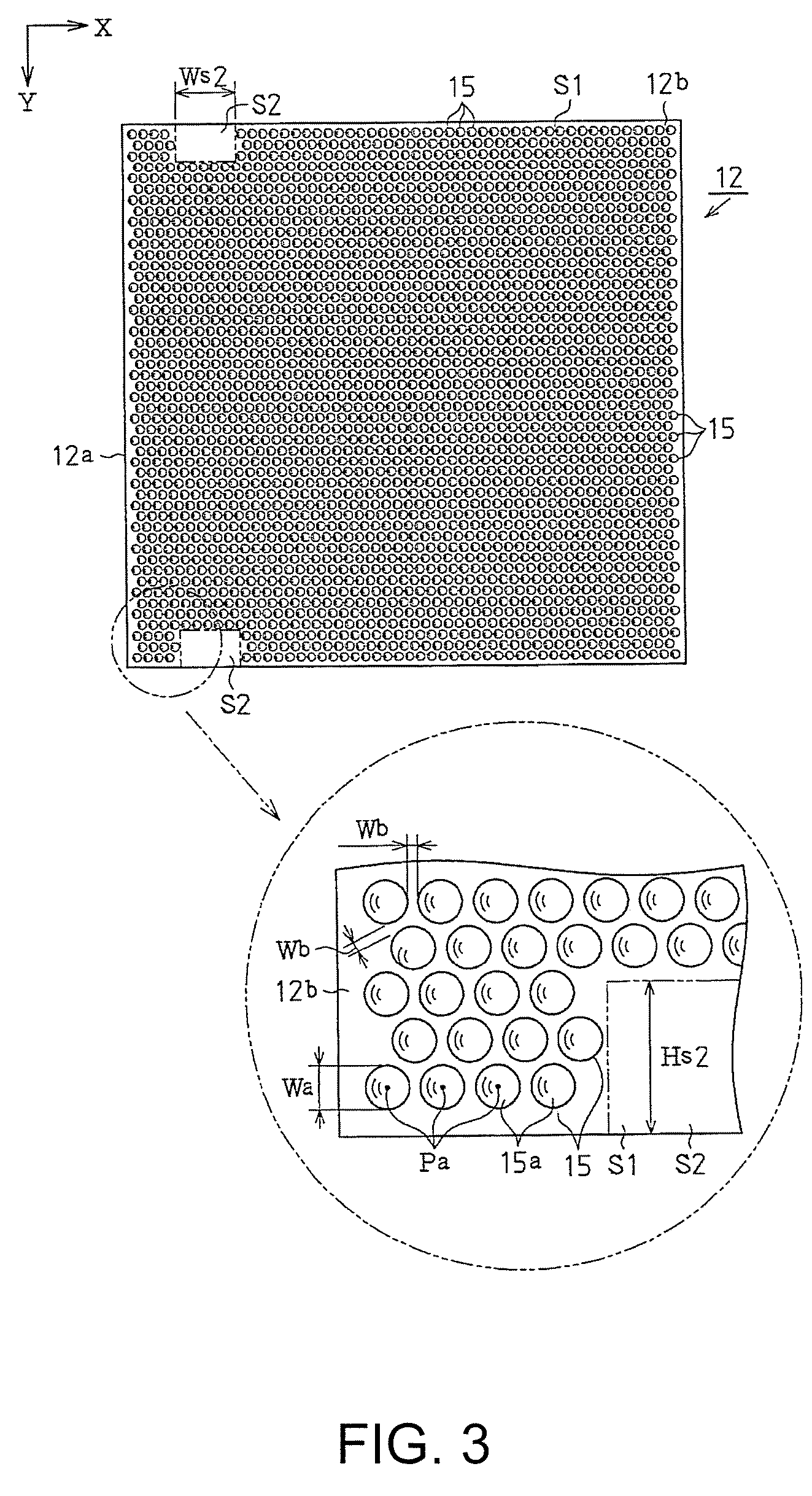
[0037]An embodiment of the invention will be described with reference to FIG. 1 through FIG. 6. First of all, a liquid crystal display device, which is a kind of electrooptical device, according to the embodiment of the invention is described. FIG. 1 is a schematic perspective view of the liquid crystal display device and FIG. 2 is a sectional view along the line A-A in FIG. 1.

[0038]As shown in FIG. 1, a liquid crystal display device 1 has a liquid crystal panel 2 and a backlight 3 which is a planar lighting device illuminating the liquid crystal panel 2 with a illumination light L.

[0039]The liquid crystal panel 2 includes a glass substrate (an opposing substrate 4) having a square plate shape and provided on the side of the backlight 3. Another glass substrate (an element substrate 5) that opposes the opposing substrate 4, and a sealing member 6 (see FIG. 2) that adheres the two glass substrates and is interposed therebetween. Liquid crystal 7 is enclosed between the opposing subst...


PUM


Abstract

An optical substrate includes an exit face through which a light entered from an incident face is emitted, a lens forming region provided on the exit face and in which a plurality of microlenses are formed, and a non-lens forming region provided in an area other than the lens forming region on the exit face and surrounded by the microlenses. The microlenses diffuse and emit the light entered through the exit face. The non-lens forming region is used to identify a predetermined direction of the substrate.

Description

BACKGROUND OF THE INVENTION[0001]1. Technical Field[0002]The present invention relates to an optical substrate, a manufacturing method thereof, a planar lighting device and an electrooptical device.[0003]2. Related Art[0004]A liquid crystal display device, which is a kind of electrooptical device, typically has a backlight which is a planar lighting device illuminating a plane and provided on the back side of a liquid crystal panel. So called edge-light type backlights are widely used for the liquid crystal display devices since it is possible to make the device thinner with the edge type backlight. In the edge type backlight, light that entered around a side face of the liquid crystal panel is led to the back side of the liquid crystal panel (to the lighting device side) and illuminates the panel.[0005]JP-A-2002-298626 is an example of related art. The edge-light type backlight typically has a light source such as a light emitting diode (LED) and a light guide plate in which the li...

Claims


Application Information

Patent Timeline
Patent Type & Authority Patents(United States)
IPC IPC(8): F21V8/00
CPCG02B6/0043G02B6/0058G02F1/133615G02B6/0065G02F2001/133354G02F1/133354G02F1/1335
Inventor HASEI, HIRONORI
Owner SEIKO EPSON CORP
Why Eureka
Try Eureka