Supercharge Your Innovation With Domain-Expert AI Agents!

Image display and display panel thereof

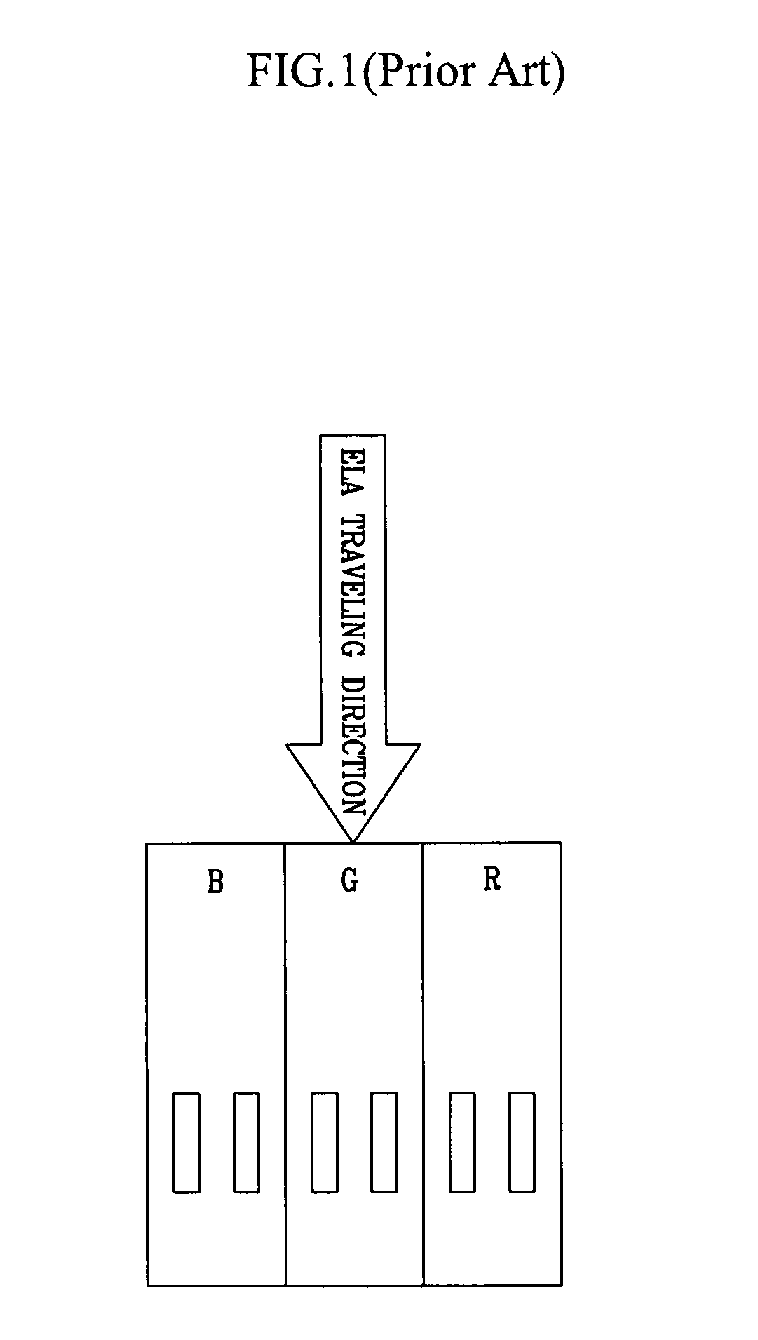
a technology which is applied in the field of image display and display panel thereof, can solve the problems of uneven luminance, current programming method has a problem of unevenness, and current programming cannot properly secure a charging time, so as to improve the illumination uniformity of each pixel in the image display

Active Publication Date: 2008-07-08
SAMSUNG DISPLAY CO LTD
View PDF33 Cites 2 Cited by
  • Summary
  • Abstract
  • Description
  • Claims
  • Application Information

AI Technical Summary

Benefits of technology

[0012]Further, luminance uniformity of each pixel in an image display may be improved using two mirror-type transistors.

Problems solved by technology

This voltage programming method has a problem of unevenness due to a variation in threshold voltages and electron mobilities of driving transistors.
However, the current programming cannot properly secure a charging time for charging loads of data lines because it should control organic EL devices with a small quantity of current.
This makes the driving transistors of the R, G, and B pixels have different characteristics, thereby resulting in unevenness of luminance.

Method used


Image

  • Image display and display panel thereof
  • Image display and display panel thereof
  • Image display and display panel thereof

Examples


Embodiment Construction

[0029]In the following detailed description, only certain exemplary embodiments of the present invention are shown and described, simply by way of illustration. As those skilled in the art would recognize, the described exemplary embodiments may be modified in various different ways, all without departing from the spirit or scope of the present invention. Accordingly, the drawings and description are to be regarded as illustrative in nature, and not restrictive. Connection of a certain part to another part may indicate that the two parts are directly coupled to each other, or that the two parts are coupled to each other through another part interposed between them.

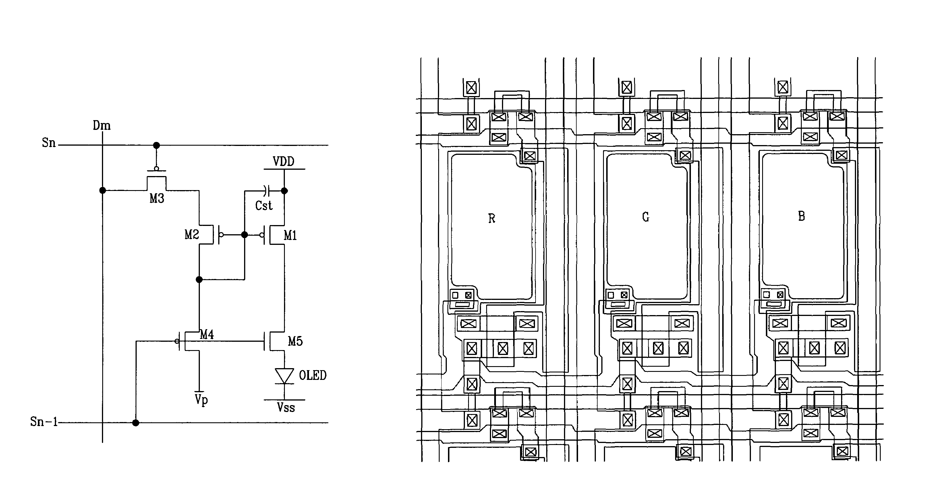
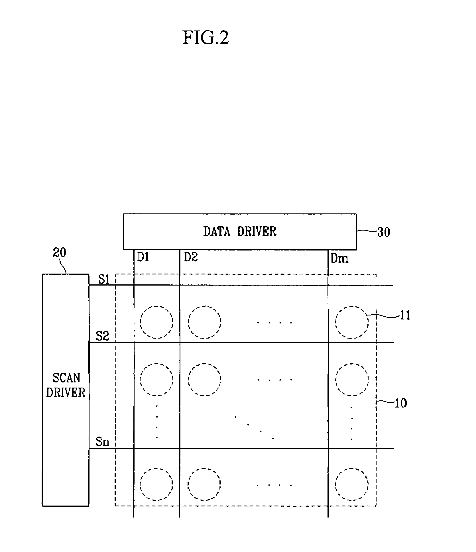
[0030]An organic EL display according to an exemplary embodiment of the present invention is explained first with reference to FIG. 2, which shows a plan view of the organic EL display according to the present invention.

[0031]As shown in FIG. 2, the organic EL display in an exemplary embodiment of the present invention inc...


PUM


Abstract

An image display and a display panel. The display panel includes data lines for transmitting a data signal corresponding to video signals, scan lines for transmitting select signals, and pixel circuits formed in pixel regions defined by two neighboring data lines and scan lines. The pixel circuit includes a display element and a first transistor having a capacitor coupled between main and control electrodes thereof. The first transistor outputs a current corresponding to the voltage between the main and control electrodes. A second transistor has a control electrode coupled to the control electrode of the first transistor. A first switch delivers the data signal from the data lines to the second transistor in response to the select signal from the current scan line.

Description

CROSS REFERENCE TO RELATED APPLICATION[0001]This application claims priority to and the benefit of Korea Patent Application No. 2003-64105 filed on Sep. 16, 2003 in the Korean Intellectual Property Office, the entire content of which is incorporated herein by reference.BACKGROUND OF THE INVENTION[0002](a) Field of the Invention[0003]The present invention relates to an image display and a display panel thereof. More specifically, the present invention relates to an organic electroluminescent (EL) display.[0004](b) Description of the Related Art[0005]In general, an organic EL display is a display that emits light by electrical excitation of fluorescent organic compound and displays images by driving each of N×M organic luminescent cells with voltages or current. The organic cell has a structure of an anode (ITO), an organic thin film, and a cathode layer (metal). The organic thin film is formed as a multi-layered structure including an emission layer (“EML”), an electron transport lay...

Claims


Application Information

Patent Timeline
Patent Type & Authority Patents(United States)
IPC IPC(8): G09G3/30H05B44/00G09G3/32H01L27/32
CPCG09G3/3233G09G2300/0819G09G2300/0842H01L27/3244G09G2310/0251G09G2320/043G09G2300/0861H10K59/12G09G3/30
Inventor SUH, MI-SOOKKIM, KEUM-NAM
Owner SAMSUNG DISPLAY CO LTD
Features
  • R&D
  • Intellectual Property
  • Life Sciences
  • Materials
  • Tech Scout
  • Unparalleled Data Quality
  • Higher Quality Content
  • 60% Fewer Hallucinations
Learn More