Methods and systems for rapid prototyping of high density circuits

a high-density circuit and rapid prototyping technology, applied in the field of rapid prototyping and methods and systems of dispensing fluid media, to achieve the effect of effective and efficien

Active Publication Date: 2008-09-02
NAT TECH & ENG SOLUTIONS OF SANDIA LLC
View PDF36 Cites 36 Cited by
  • Summary
  • Abstract
  • Description
  • Claims
  • Application Information

AI Technical Summary

Benefits of technology

[0010]A preferred embodiment provides, for example, systems and methods of combining DW technologies with stereolithography (SL). Accordingly, existing SL systems that fabricate a subject part layer by layer are combined with DW technologies that deposit whatever material required for a particular application. SL fabricated parts may now have, for example, complex three-dimensional (3D) embedded circuitry within the fabricated part by DW technology. Thus, the systems and methods disclosed herein provide for increased micro-fabrication and micro-stereolithography.
[0011]Another preferred embodiment provides, for example, rapid development of circuitry to manufacture more compact components that provide advantages such as weight savings, self-assembly components, rapid manufacturing, micro-fabrication, micro-stereolithography and micro-circuitry for aerospace, space, homeland security, national defense and a variety of other applications.
[0012]Still another preferred embodiment provides, for example, a system and method of integrating thermally curable media with SL without the need for intermediate washing, curing and / or drying. Thus, the systems and methods disclosed herein could easily be converted to make complex, 3D embedded circuitry, for example, without the addition of costly equipment.
[0013]Yet another preferred embodiment provides a system and method for Rapid Prototyping High Density Circuit (RPHDC) manufacturing of solderless connectors and pilot devices with terminal geometries that are compatible with DW mechanisms and reduce contact resistance where the electrical system is encapsulated within structural members and manual electrical connections are eliminated in favor of automated DW traces.

Problems solved by technology

SL fabricated parts may now have, for example, complex three-dimensional (3D) embedded circuitry within the fabricated part by DW technology.

Method used


Image

  • Methods and systems for rapid prototyping of high density circuits
  • Methods and systems for rapid prototyping of high density circuits
  • Methods and systems for rapid prototyping of high density circuits

Examples


example

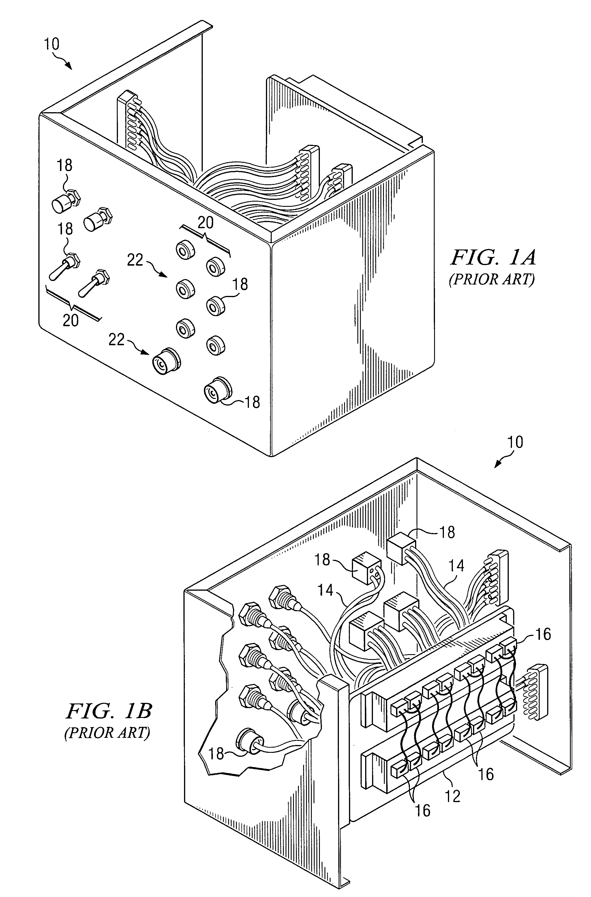
[0030]Modern low voltage distribution networks, for example, contain an enclosure 10 comprising junction boxes or load centers 12 where bundles of conductors 14 are routed to exposed terminals 16, as depicted for example in FIGS. 1A and 1B, and pilot devices (not shown). Such enclosures 10 must be designed to prevent unnecessary compression of the wiring which can lead to, for example, insulation failures and short circuits. Enclosures 10 known in the art are typically made from sheet metal and are relatively bulky in size. For example the network of load centers 12 and conductors 14 depicted in FIGS. 1A and 1B, may have signals typically ranging from 6 to 28 volts. The depicted network has load centers 12 and conductors 14 routed and switched to connectors 18 on three sides of the enclosure 10. For a network of this size and complexity, it is typical to utilize an enclosure 10 with dimensions of, for example, 12.7 cm.×15.2 cm.×10.2 cm.

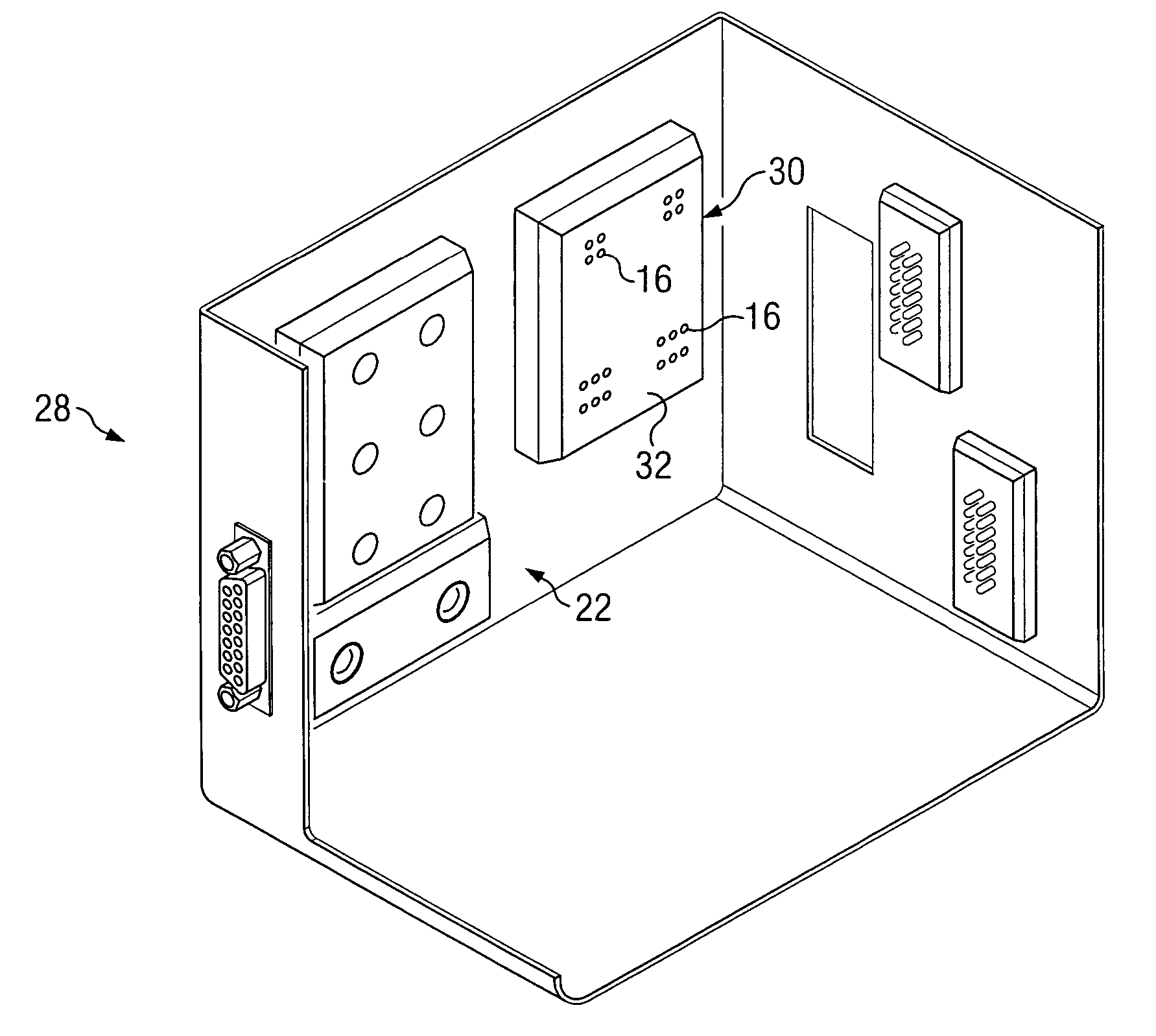
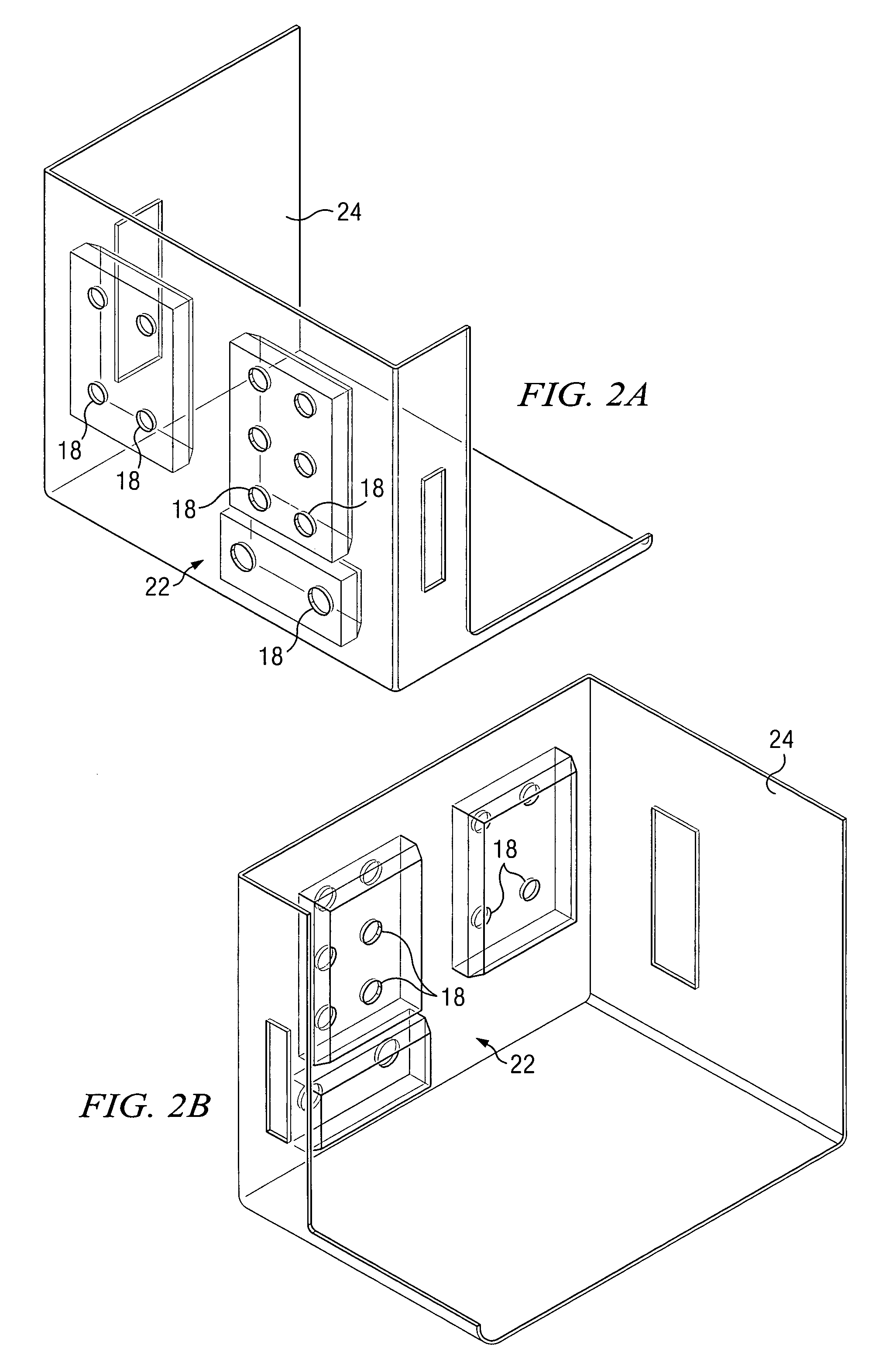
[0031]The prior art enclosure 10 depicted in FI...


PUM

PropertyMeasurementUnit
sizeaaaaaaaaaa
thicknessaaaaaaaaaa
displacement testsaaaaaaaaaa

Abstract

A preferred embodiment provides, for example, a system and method of integrating fluid media dispensing technology such as direct-write (DW) technologies with rapid prototyping (RP) technologies such as stereolithography (SL) to provide increased micro-fabrication and micro-stereolithography. A preferred embodiment of the present invention also provides, for example, a system and method for Rapid Prototyping High Density Circuit (RPHDC) manufacturing of solderless connectors and pilot devices with terminal geometries that are compatible with DW mechanisms and reduce contact resistance where the electrical system is encapsulated within structural members and manual electrical connections are eliminated in favor of automated DW traces. A preferred embodiment further provides, for example, a method of rapid prototyping comprising: fabricating a part layer using stereolithography and depositing thermally curable media onto the part layer using a fluid dispensing apparatus.

Description

GOVERNMENT INTEREST STATEMENT[0001]This invention was developed under Contract DE-AC04-94AL85000 between Sandia Corporation and the U.S. Department of Energy. The U.S. Department of Energy has certain rights to this invention.BACKGROUND[0002]The present invention relates to the general field of rapid prototyping (RP), and methods and systems of dispensing fluid media such as direct-write (DW) technologies.[0003]RP technologies, also known as Solid Freeform Fabrication (SFF), layered manufacturing and other similar technologies enable the manufacture of complex three-dimensional (3D) parts. RP technologies, in particular, generally construct parts by building one layer at a time for use in, for example, the toy, automotive, aircraft and medical industries. Oftentimes prototypes made by RP technologies aid in research and development and provide a low cost alternative to traditional prototyping.[0004]Stereolithography (SL) is one of the most widely used RP technologies known in the ar...

Claims


Application Information

Patent Timeline
Patent Type & Authority Patents(United States)
IPC IPC(8): B29C35/04
CPCB29C67/0059B29C67/0092B29C67/0066B29C64/112B29C64/135B29C64/40B33Y70/00B33Y10/00
Inventor PALMER, JEREMY A.DAVIS, DONALD W.CHAVEZ, BART D.GALLEGOS, PHILLIP L.WICKER, RYAN B.MEDINA, FRANCISCO R.
Owner NAT TECH & ENG SOLUTIONS OF SANDIA LLC
Why Eureka
Try Eureka