

Semiconductor device
- Summary
- Abstract
- Description
- Claims
- Application Information
AI Technical Summary
Benefits of technology
Problems solved by technology
Method used
Image

Examples
first embodiment
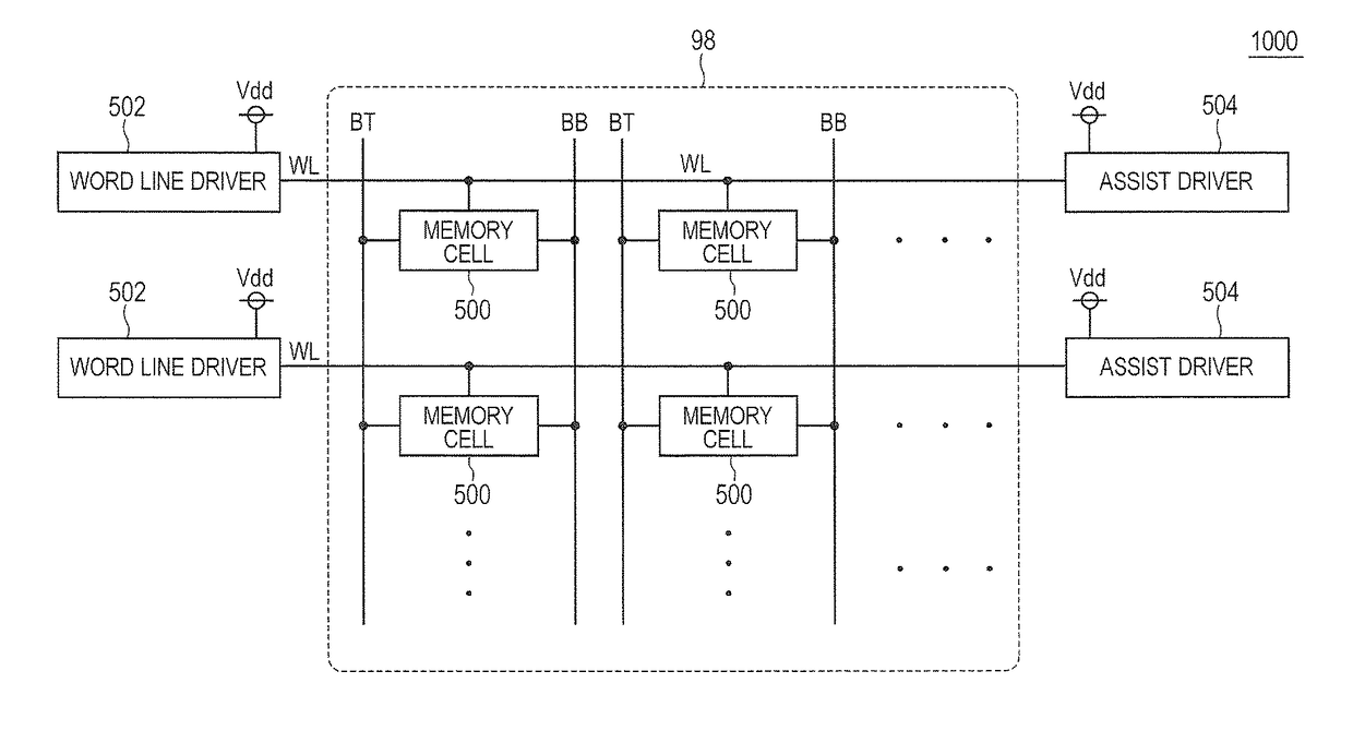
[0018]FIG. 1 is a diagram illustrating a configuration of a semiconductor device of a first embodiment.
[0019]Refer to FIG. 1, this semiconductor device 1000 includes a memory array 98, a plurality of word lines WL, a plurality of bit line pairs BT and BB, a plurality of word line drivers 502, a first power source Vdd, and a plurality of assist drivers 504.
[0020]The memory array 98 includes a plurality of memory cells 500 arranged in matrix.
[0021]The word lines WL are provided and correspond respectively to the rows of the memory array 98. The word lines WL are coupled to the memory cells 500 of the corresponding rows.
[0022]The bit line pair BT and BB is provided and corresponds respectively to the columns of the memory array 98. The bit line pair BT and BB is coupled to the memory cells 500 of the corresponding columns.
[0023]The word line drivers 502 are coupled to one ends of the word lines WL. When a corresponding row is selected, one end of the word line WL is coupled to the firs...
second embodiment
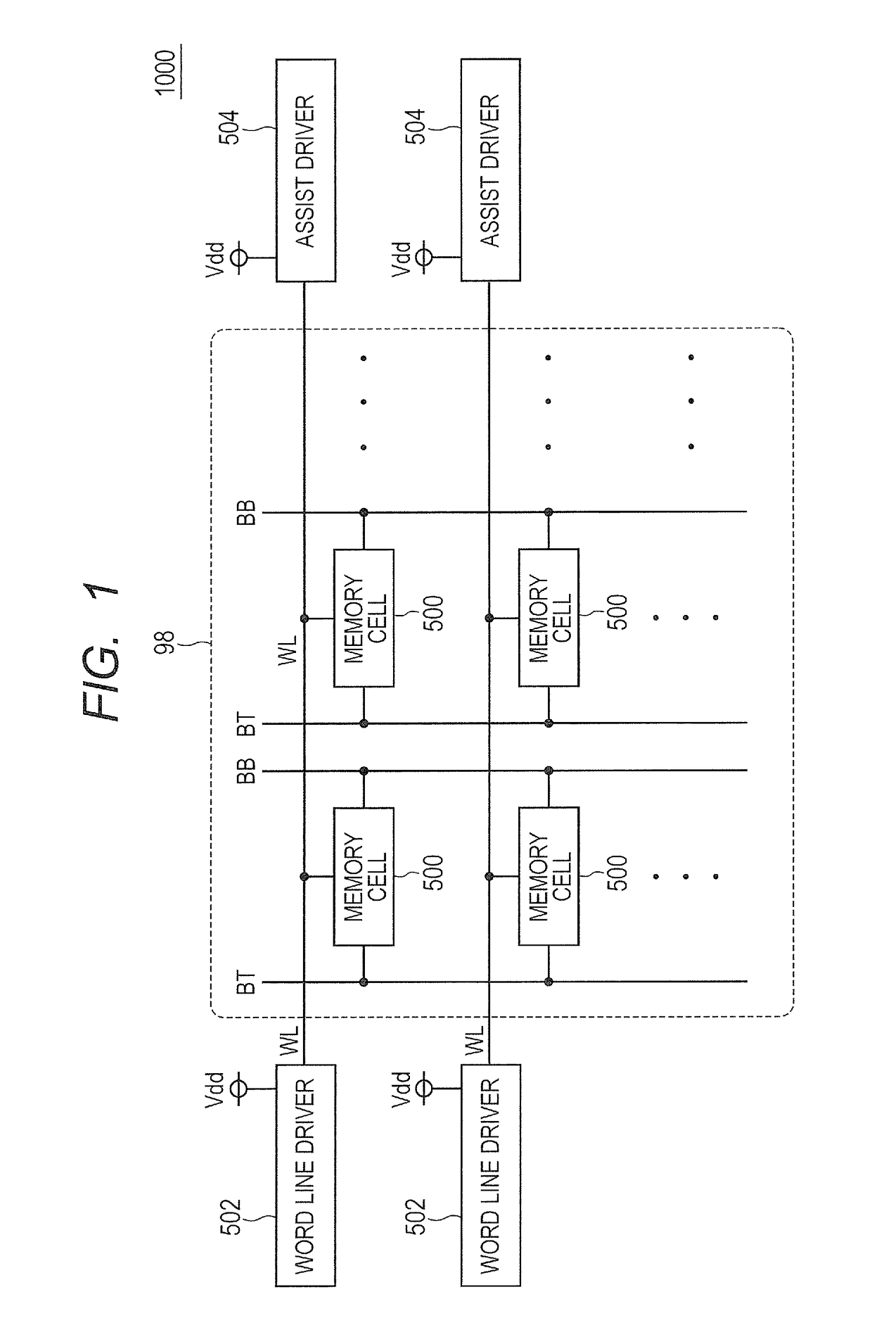
[0026]FIG. 2 is a diagram illustrating a configuration of a semiconductor device of a second embodiment.
[0027]A semiconductor device 100 includes a memory array 62, a plurality of word lines WL, a plurality of bit line pairs BT and BB, a plurality of word line drivers 22, a plurality of assist drivers 10, a plurality of column selectors 4, a plurality of pre-charge circuits 3, a control circuit / address decoder 21, a plurality of write drivers 5, and a plurality of sense amplifiers 6.
[0028]The memory array 62 includes a plurality of memory cells 1 arranged in matrix. In FIG. 2, the memory cells 1 are represented in the form of two rows and two columns. The memory cells 1 are SRAM (Static Random Access Memory) cells.
[0029]Each of the memory cells 1 includes PMOS (Metal-Oxide-Semiconductor) transistors P1 and P2 as load transistors, NMOS transistors N1 and N2 as driver transistors, and NMOS transistors N20 and N21 as access transistors.
[0030]The sources of the load transistors P1 and P...
third embodiment
[0068]FIG. 4 is a diagram illustrating a configuration of a semiconductor device of a third embodiment.
[0069]Descriptions will now be made to any of those differences of a semiconductor device 200 of FIG. 4 from the semiconductor device 100 of FIG. 2.
[0070]The assist control circuit 12 includes two stages of inverters IV4 and IV5.
[0071]The control circuit / address decoder 21 transmits a control signal pulse PL to the assist control circuit 12 and an assist driver 11, through a signal wiring LA. The signal wiring LA is provided outside the memory array 62, in a direction horizontal to the substrate where the semiconductor device 200 is implemented.
[0072]The inverter IV4 receives a control signal pulse PL from the control circuit / address decoder 21. The inverter IV5 receives an output from the inverter IV4.
[0073]The assist driver 11 includes a NAND circuit NAN2 and a PMOST transistor P8.
[0074]The PMOS transistor P8 is provided between the terminal end Y of the word line WL and the powe...
PUM
 Abstract
Description
Claims
Application Information