Circuits and methods for repairing defects in memory devices

a memory device and circuit technology, applied in the field of circuits and methods for repairing defects in memory devices, can solve problems such as the dumping of the entire memory device, and achieve the effect of saving power

Active Publication Date: 2008-10-14
MICRON TECH INC
View PDF20 Cites 10 Cited by
  • Summary
  • Abstract
  • Description
  • Claims
  • Application Information

AI Technical Summary

Problems solved by technology

Some defects are irreparable, causing the entire memory device to be discarded.

Method used


Image

  • Circuits and methods for repairing defects in memory devices
  • Circuits and methods for repairing defects in memory devices
  • Circuits and methods for repairing defects in memory devices

Examples


Embodiment Construction

[0020]The following description and the drawings illustrate specific embodiments of the invention sufficiently to enable those skilled in the art to practice it. Other embodiments may incorporate structural, logical, electrical, process, and other changes. In the drawings, like numerals describe substantially similar components throughout the several views. Examples merely typify possible variations. Portions and features of some embodiments may be included in or substituted for those of others. The scope of the invention encompasses the full ambit of the claims and all available equivalents.

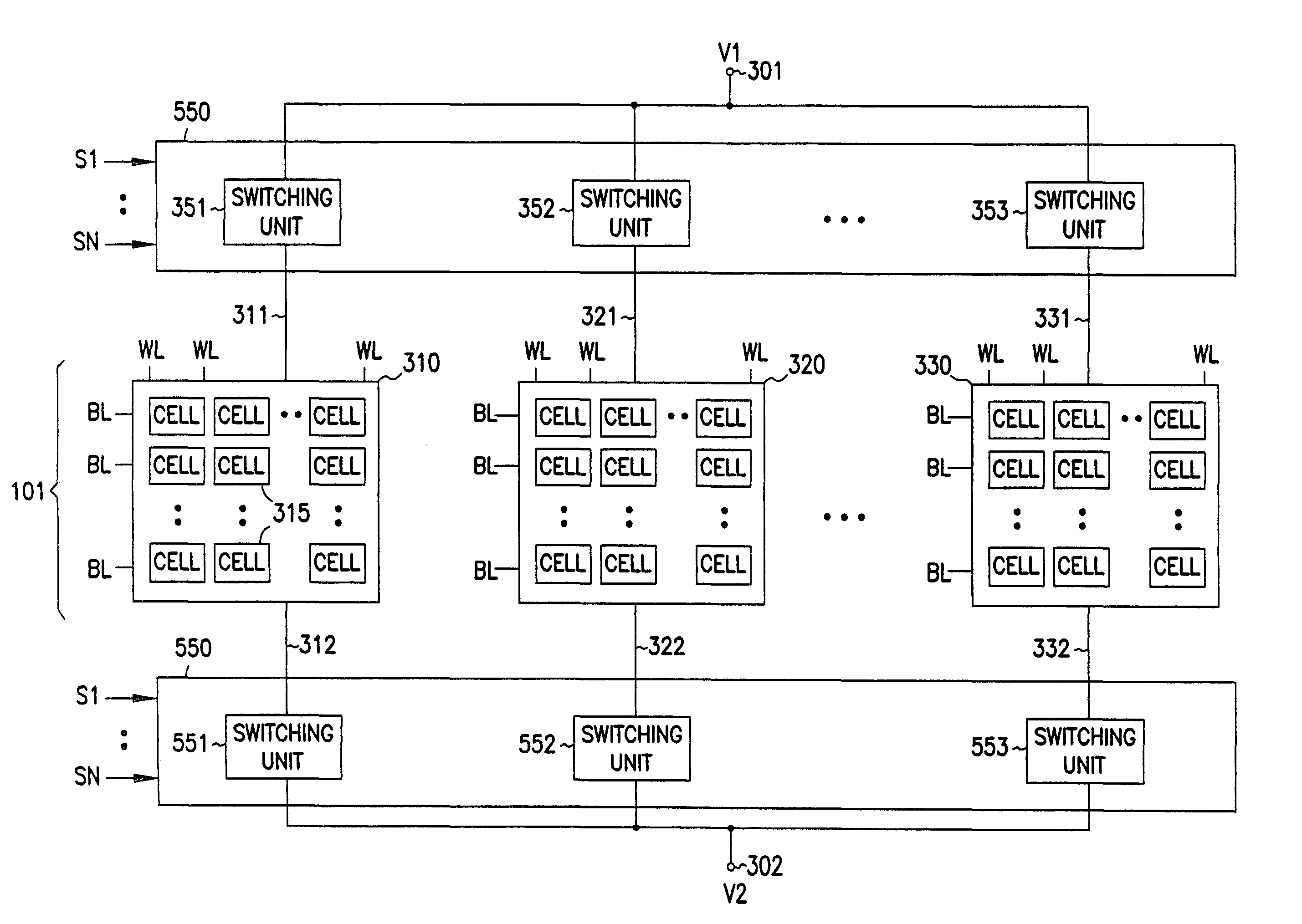
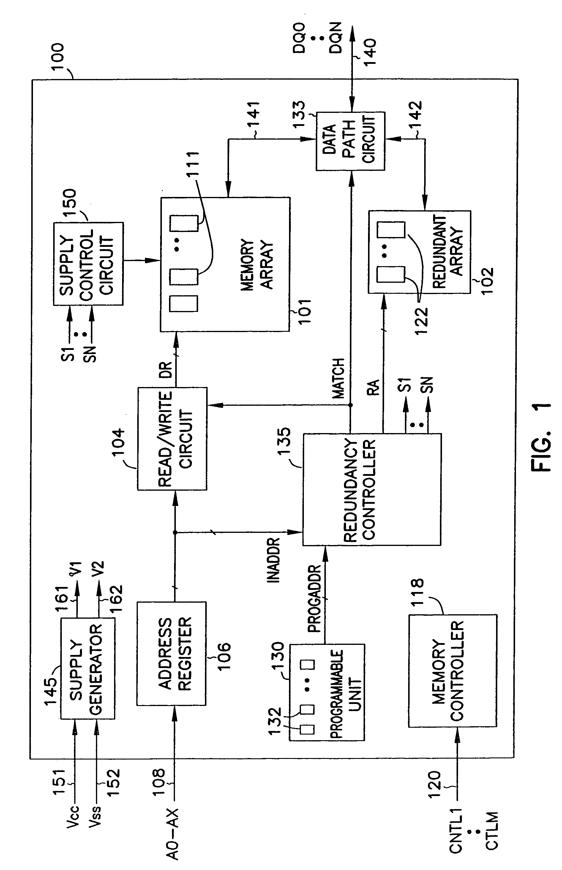
[0021]FIG. 1 shows a memory device according to an embodiment of the invention. Memory device 100 includes a memory array 101 and a redundant array 102. Memory array 101 includes a number of memory segments 111. Redundant array 102 includes a plurality of redundant segments 122. Each of the redundant segments 122 can replace a defective memory segment among memory segments 111.

[0022]A read / write...


PUM


Abstract

A memory device has a number of memory segments connected to a supply source through a supply control circuit. If one of the memory segments is defective, the supply control circuit isolates the defective memory segment from the supply source. The memory device replaces the defective memory segment with a redundant segment.

Description

FIELD OF INVENTION[0001]The present invention relates generally to semiconductor devices, more particularly to repairing defects in memory devices.BACKGROUND[0002]Memory devices reside in many computers and electronic products to store data.[0003]A typical memory device has many memory cells and some redundant (spare) cells. When some of the memory cells are defective, the defective memory cells can be replaced with redundant cells to repair the memory device. This repairing method saves the entire memory device when only a few memory cells are defective.[0004]Certain defects are repairable. Some defects are irreparable, causing the entire memory device to be discarded.SUMMARY OF THE INVENTION[0005]The present invention provides techniques for repairing defects in memory devices. Various embodiments of the invention provide circuits and methods for repairing circuit shorts involving supply nodes in memory devices.[0006]One aspect includes a memory device having a memory array connec...

Claims


Application Information

Patent Timeline
Patent Type & Authority Patents(United States)
IPC IPC(8): G11C29/00G11C7/00H02H3/05
CPCG11C29/83G11C29/832
Inventor MARR, KENNETH W.
Owner MICRON TECH INC
Why Eureka
Try Eureka