Technique for memory imprint reliability improvement

a technology of memory imprint and reliability improvement, applied in the field of memory array imprint reduction, can solve the problems of requiring reliability to address new problems based on non-traditional parameters, bring new challenges,

Active Publication Date: 2013-07-23
TEXAS INSTR INC
View PDF10 Cites 392 Cited by
  • Summary
  • Abstract
  • Description
  • Claims
  • Application Information

AI Technical Summary

Problems solved by technology

Memory is an important aspect of power consumption.
While each of these new technologies brings new advantages, they also bring new challenges.
In particular, they require reliability to address new problems based upon non-traditional parameters.

Method used


Image

  • Technique for memory imprint reliability improvement
  • Technique for memory imprint reliability improvement
  • Technique for memory imprint reliability improvement

Examples


Embodiment Construction

[0026]The present invention will now be described with reference to the attached drawing figures, wherein like reference numerals are used to refer to like elements throughout, and wherein the illustrated structures and devices are not necessarily drawn to scale.

[0027]Also, it will be appreciated that the method and memory devices disclosed may be applied to a wide variety of memory devices. For example, memory devices may include memory cells having ferroelectric capacitive elements or other elements that may be affected by imprint or memory devices that may be impacted by signal margin.

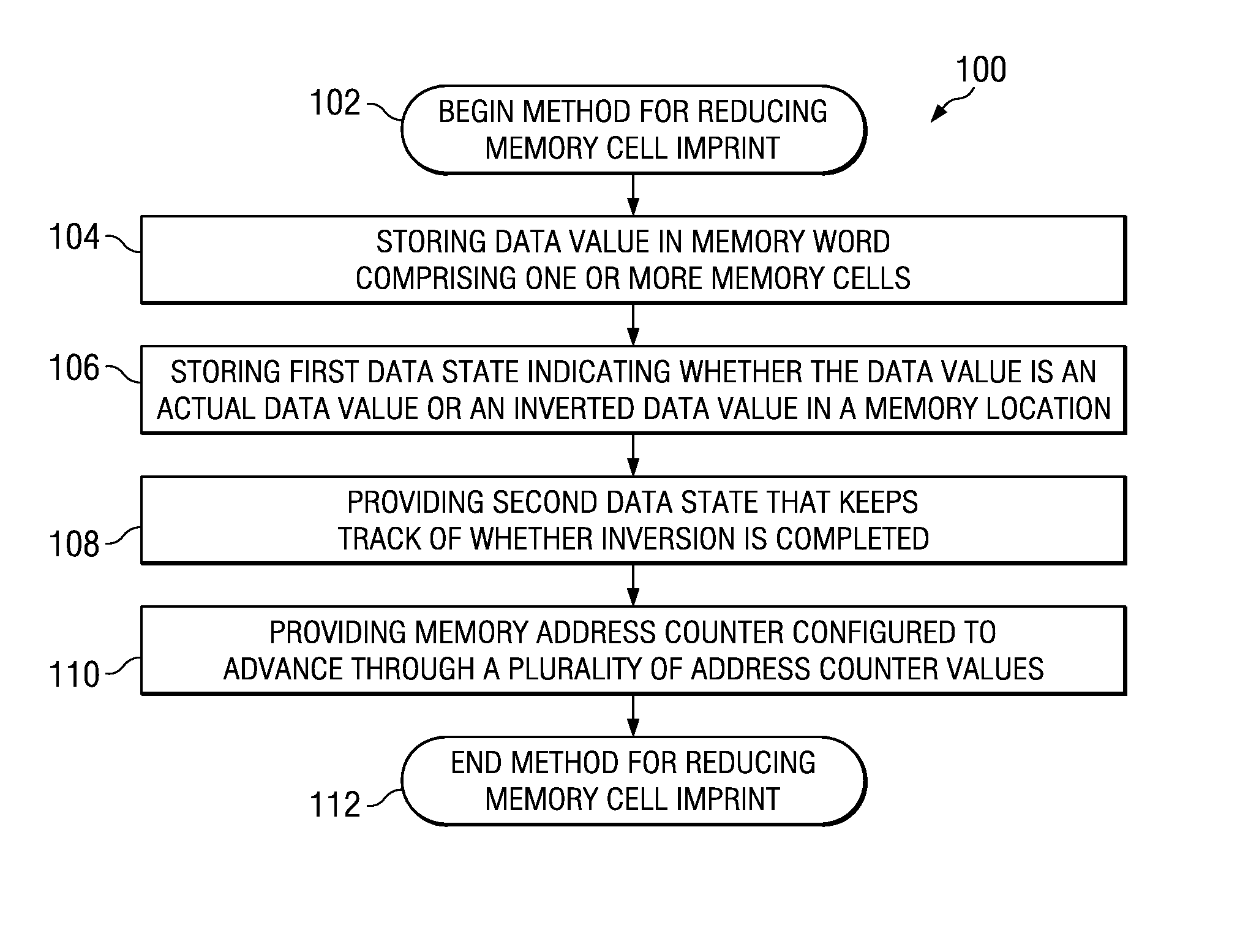
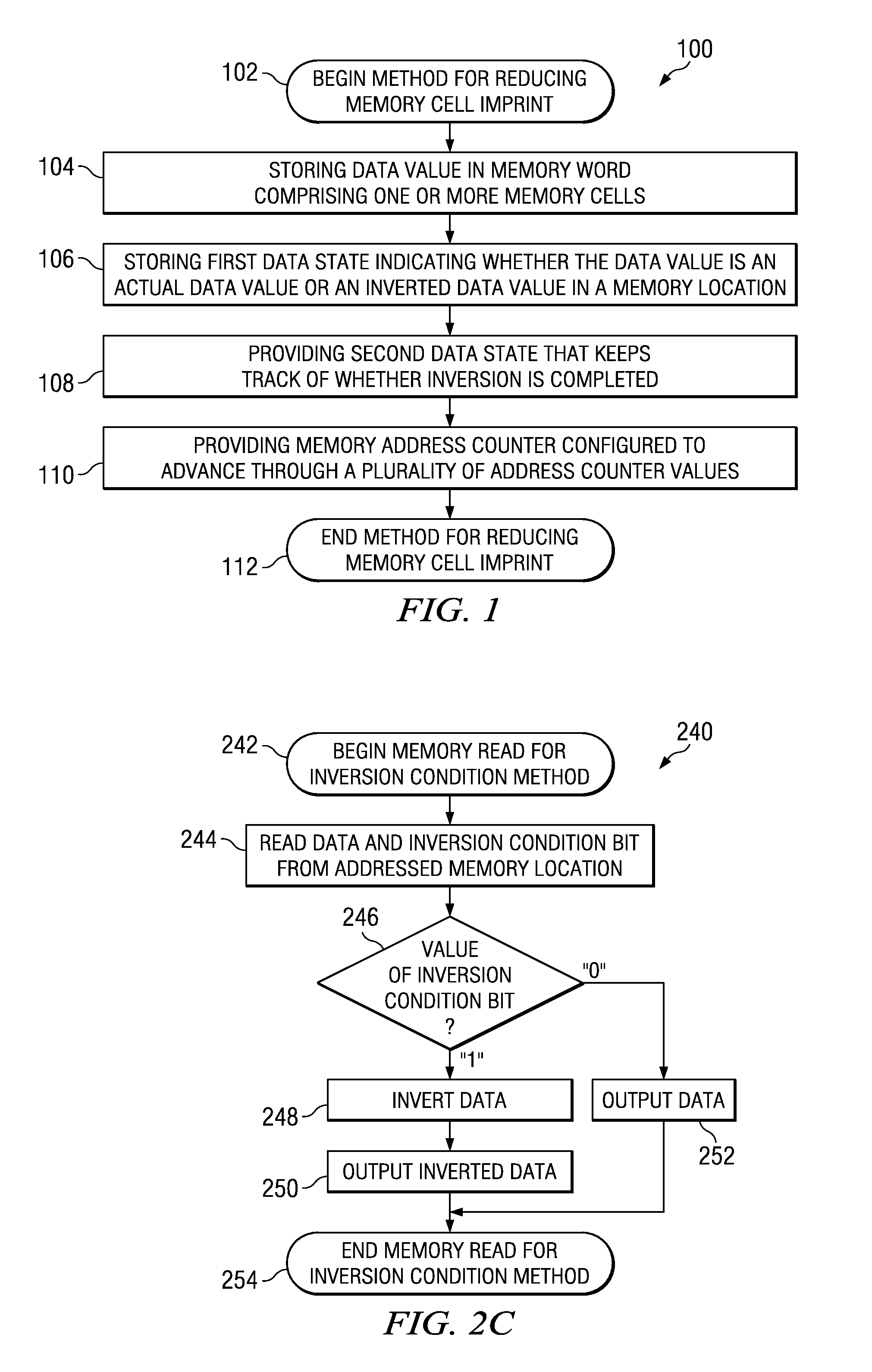
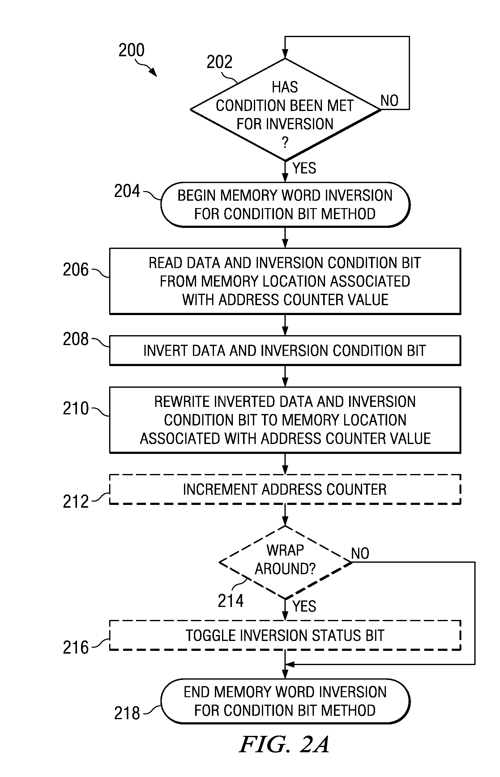
[0028]As provided herein the present invention relates a method and system for improving the reliability of electronic memory by for reducing imprint of memory cells. More particularly, a bit (e.g., an inversion condition bit, an inversion status bit) is associated with a data value (i.e., a value of the “user data” read from, or to be written to, a memory word or location) comprised within a memory...


PUM


Abstract

One embodiment of the present invention relates to a method of reducing imprint of a memory cell. The method comprises adding an inversion condition bit operably associated with one or more memory cells storing a memory word. The inversion condition bit indicates whether the memory word represents an actual payload or an inversion of the actual payload. The inversion condition bit and memory word are selectively toggled by a control circuitry. Inversion is performed by reading the inversion condition bit and memory word and rewriting the memory word back to the one or more memory cells in an inverted or non-inverted state, depending on an inversion condition bit. The inversion condition bit is then written to the inversion status bit value. The memory address is incremented, and the inversion status data state is toggled once the address counter addresses the entire memory array. Other methods and circuits are also disclosed.

Description

RELATED APPLICATION[0001]This application claims priority to Ser. No. 61 / 017,381 filed Dec. 28, 2007, which is entitled “Technique for Memory Imprint Reliability Improvement”.FIELD OF INVENTION[0002]The present invention relates generally to semiconductor devices and more particularly to reduction of imprint for memory arrays with low impact on memory system availability.BACKGROUND OF THE INVENTION[0003]In recent years the market of the semiconductor industry has grown considerably for supplying integrated chips to companies which manufacture portable electronic devices. The integrated chips used to make these portable electronic devices, such as cell phones, PDAs, laptop computers and the like, are mostly made in emerging technology nodes. This is because emerging technology nodes offer higher density chips with greater performance and lower power consumption. These qualities are important to portable electronic devices which are continually striving to offer greater functionality ...

Claims


Application Information

Patent Timeline
Patent Type & Authority Patents(United States)
IPC IPC(8): G11C29/00
CPCG06F11/1008G11C7/1006H03M13/19H03M13/451G06F11/1076G06F11/108
Inventor ROINE, PER TORSTEIN
Owner TEXAS INSTR INC
Why Eureka
Try Eureka