Semiconductor memory device and method of operating the same

a memory device and semiconductor technology, applied in the field of semiconductor memory devices, can solve the problems of increasing current degradation, increasing the level of erase voltage supplied for erase operation, and increasing the level of erase verification level, so as to minimize the deterioration of physical and electrical properties of the memory device and improve the reliability of operation.

Active Publication Date: 2013-09-03
SK HYNIX INC
View PDF17 Cites 387 Cited by
  • Summary
  • Abstract
  • Description
  • Claims
  • Application Information

AI Technical Summary

Benefits of technology

[0010]Exemplary embodiments relate to a semiconductor memory device and a method of operating the same, which are capable of minimizing the deterioration of physical and electrical properties of the memory device resulting from repeated program and erase operations and capable of improving reliability of the operation by differently setting conditions for sensing data (or threshold voltage) of a memory cell.

Problems solved by technology

Meanwhile, with an increase in the number of program and erase cycles, the influence of current degradation is increased and so an erase verification level gradually shows a downward tendency.
When the erase verification level gradually falls, the level of an erase voltage supplied for the erase operation gradually rises, and the electrical properties of a memory cell are deteriorated.

Method used


Image

  • Semiconductor memory device and method of operating the same
  • Semiconductor memory device and method of operating the same
  • Semiconductor memory device and method of operating the same

Examples


Embodiment Construction

[0033]Hereinafter, some exemplary embodiments of the present disclosure will be described in detail with reference to the accompanying drawings. The figures are provided to allow those having ordinary skill in the art to understand the scope of the embodiments of the disclosure.

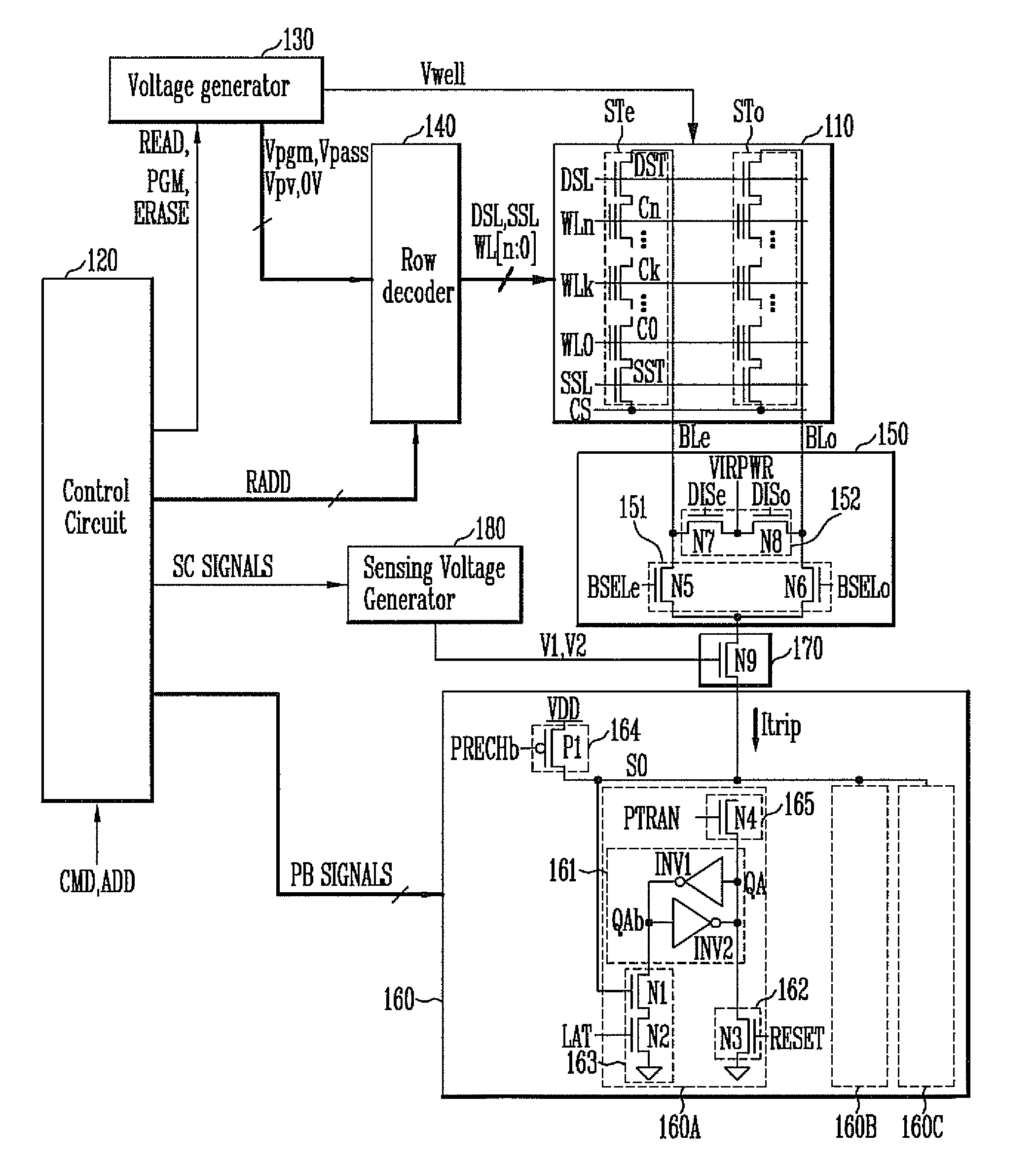
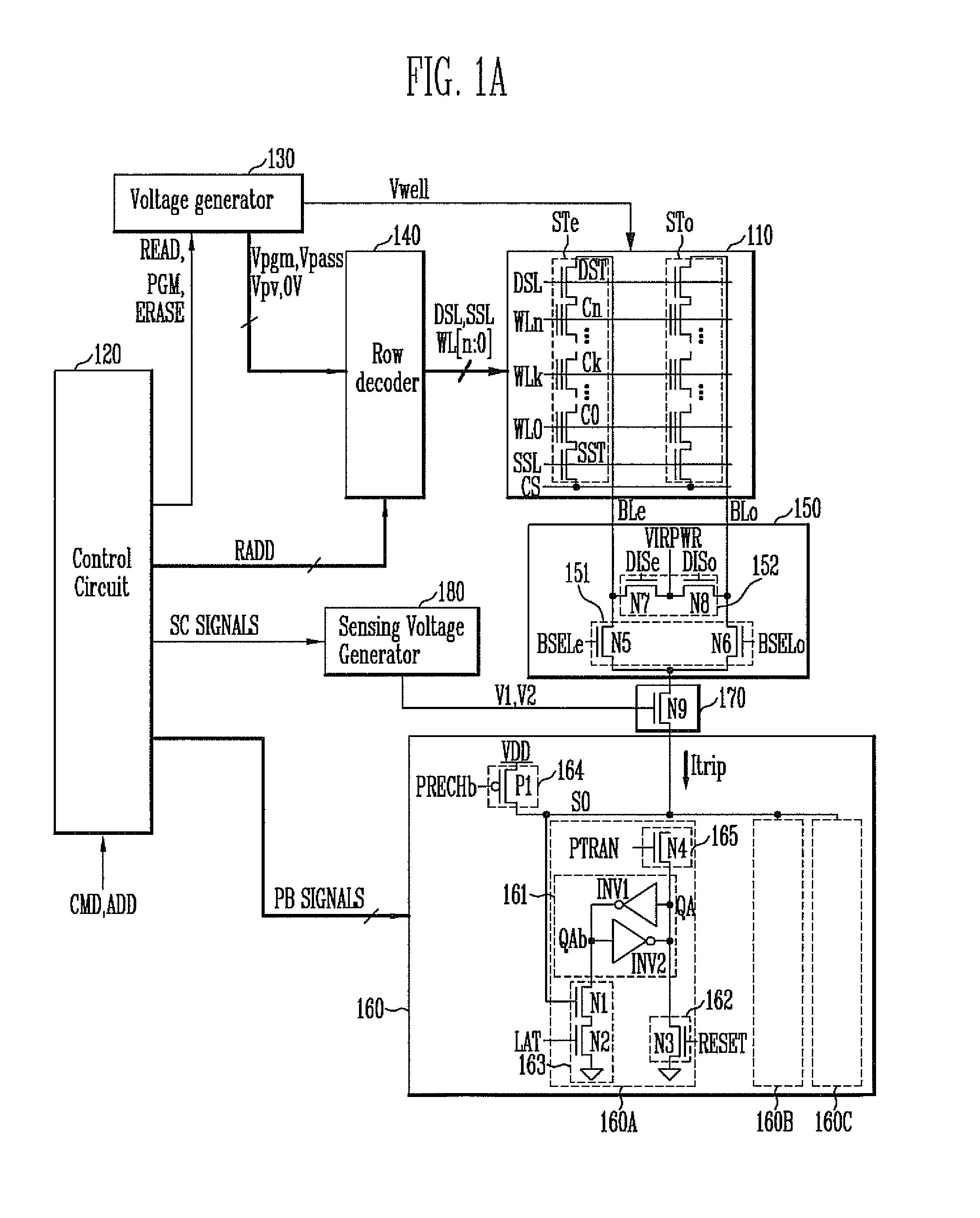
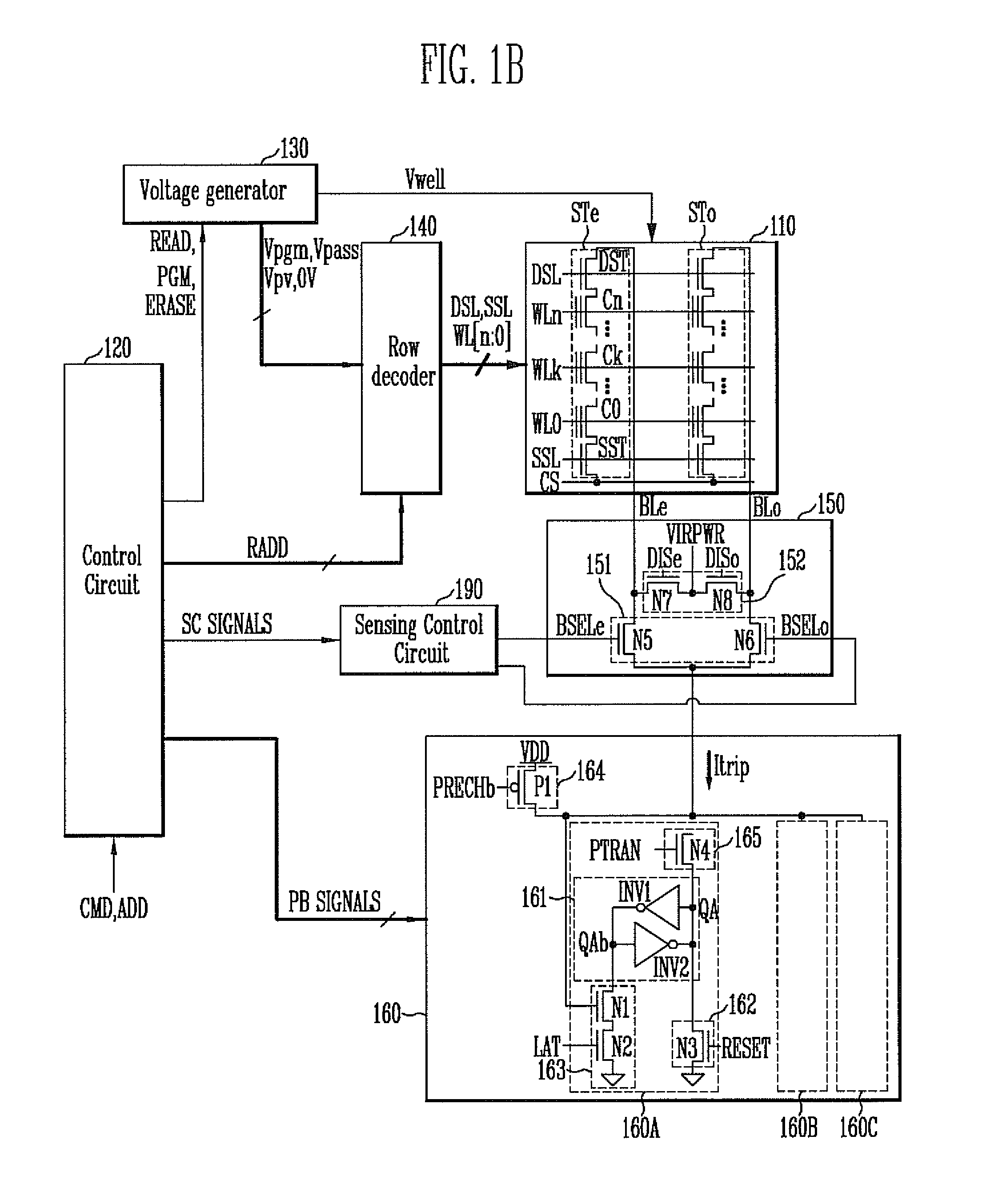
[0034]FIGS. 1A and 1B are diagrams illustrating a semiconductor memory device according to the present disclosure.

[0035]Referring to FIG. 1A, the semiconductor memory device includes a memory array 110, a control circuit 120, a voltage supply circuit (130, 140), a bit line selection circuit 150, a page buffer 160, and a sensing control circuit (170 and 180).

[0036]The memory array 110 may include a plurality of memory blocks. Each of the memory blocks is coupled to bit lines BLe and BLo, and includes memory strings STe and STo coupled in parallel to a common source line CS. For convenience, only one memory block, including the two memory strings STe and STo are shown in FIG. 1A.

[0037]Each (for example, STe) of...


PUM


Abstract

A semiconductor memory device includes a memory string coupled to a bit line, a page buffer configured to sense a sensing current of the bit line in an erase verification operation or a program verification operation, and a sensing control circuit configured to differently set a level of the sensing current in the erase verification operation and the program verification operation in order to sense the threshold voltage level of a selected memory cell of the memory string.

Description

CROSS-REFERENCE TO RELATED APPLICATION[0001]Priority to Korean patent application number 10-2010-0039897 filed on Apr. 29, 2010, the entire disclosure of which is incorporated by reference herein, is claimed.BACKGROUND[0002]Exemplary embodiments relate to a semiconductor memory device and a method of operating the same and, more particularly, to a semiconductor memory device and a method of operating the same, which are capable of optimizing operating conditions.[0003]A semiconductor memory device receives and stores data. In nonvolatile memory devices, such as flash memory, data is stored through a program operation, data is deleted through an erase operation, and data is outputted through a read operation.[0004]In the flash memory device, the threshold voltage level of a memory cell is shifted according to data stored in the memory cell. That is, the threshold voltage of a memory cell is shifted through a program operation or an erase operation. In order to check whether the thres...

Claims


Application Information

Patent Timeline
Patent Type & Authority Patents(United States)
IPC IPC(8): G11C16/06G11C16/04
CPCG11C16/26G11C16/344
Inventor KIM, HYUNG SEOK
Owner SK HYNIX INC
Why Eureka
Try Eureka