Closely spaced electrodes with a uniform gap

a gap and electrode technology, applied in the field of diodes, thermionic, tunneling, can solve the problems of low conversion efficiency, limited operation, and limited cooling measurement in the working apparatus, and achieve the effects of low cost and mass production, simple and inexpensive thermo-tunneling, and low cos

Inactive Publication Date: 2008-11-25
TEMPRONICS INC
View PDF16 Cites 18 Cited by
  • Summary
  • Abstract
  • Description
  • Claims
  • Application Information

AI Technical Summary

Benefits of technology

[0038]The disclosure provides a way for electrode materials to be brought together in a new, unobvious manner to produce a simple and inexpensive thermo-tunneling or thermionic device which has the following advantages: (1) simplicity by eliminating the need for actuators and control systems required by the prior art, (2) making use of the technology and manufacturing processes already developed in the electric light bulb and semiconductor industries to achieve low cost and mass production, (3) achieving the narrow spacing gaps between electrodes without the use of spacers so as to permit tunneling of hot electrons from one electrode to the other thereby cooling the first electrode, and (4) maintaining a uniform spacing gap over large electrode areas such as one square centimeter.

Problems solved by technology

Because of the limitations imposed by the relatively large physical spacing available, these diodes needed to operate at a very high temperature (greater than 1000 degrees Kelvin).
The maintenance of separation of the electrodes at atomic dimensions over a large area has been the single, most significant challenge in building devices that can remove heat from a conductor.
The scanning tunneling microscope, for example, requires a special lab environment that is vibration free, and its operation is limited to an area of a few square nanometers.
Even very recently, all measurements of cooling in a working apparatus have been limited to an area of a few square nanometers.
Furthermore, heat and other stresses can cause changes in warping and bending over time, presenting a further challenge in maintaining uniform separation once achieved.
The state of the art of a tunneling energy conversion device suffers from one or more of the following limitations: (1) a separation that is too large for tunneling, (2) an area that is too small for significant energy conversion, (3) layers of solid material that cannot be thermally isolated resulting in low conversion efficiency, and (4) a design that is too complex to manufacture cost effectively.
A separation of 10 microns or more has been achieved by many thermionic systems, but these systems only operate at very high temperatures, require a costly design for safety, and are limited to environments where this temperature is achieved.
Such area was too small (compared to the desired area of about one square centimeter or more) to allow enough current to flow through, even in the most optimal of materials, to convert significant energy.
However, these methods all require solid materials to be in contact with each other in layers.
The heat flows easily from layer to layer, limiting the temperature difference and the conversion efficiency.
Because the two electrodes are in contact, the design is at the mercy of available thermoelectrically sensitive materials, and the energy barrier for the electrons to traverse cannot be arbitrarily configured, as is possible by setting the width of a vacuum gap.
The materials having needed properties are exotic and expensive elements like bismuth and telluride.
For these reasons, thermoelectric devices are limited to a high cost per watt of cooling power and a low efficiency of about 7 percent.
Because of the elaborate processes involved in shaping one surface against the other and the use of multiple feedback control systems to maintain parallelism, this design approach is a challenge to manufacture at a low cost.
These three methods are either susceptible to post-fabrication fluctuations due to warping or thermal expansion differences between the electrodes, or require the array of actuators to compensate for these fluctuations.
One disadvantage of these dielectric spacers is that they conduct heat from one electrode to the other, reducing the efficiency of the conversion process.
Another disadvantage of this method is that the flexible metal electrodes can stretch or deform between the spacers over time in the presence of the large electrostatic forces and migrate slowly toward a spacing that permits conduction rather than tunneling or thermionic emission.
There remain continuing and difficult challenges in meeting the requirements for achieving and maintaining electrode spacing at less than 20.0 nanometer separation gaps, and in mass-producing low cost thermo-tunneling devices, in spite of efforts to date.

Method used


Image

  • Closely spaced electrodes with a uniform gap
  • Closely spaced electrodes with a uniform gap
  • Closely spaced electrodes with a uniform gap

Examples


example 1

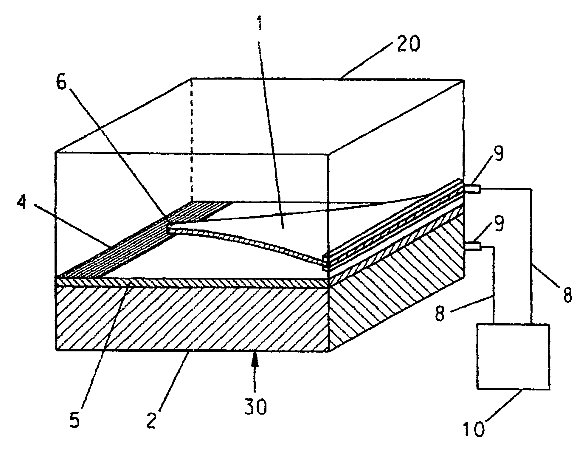
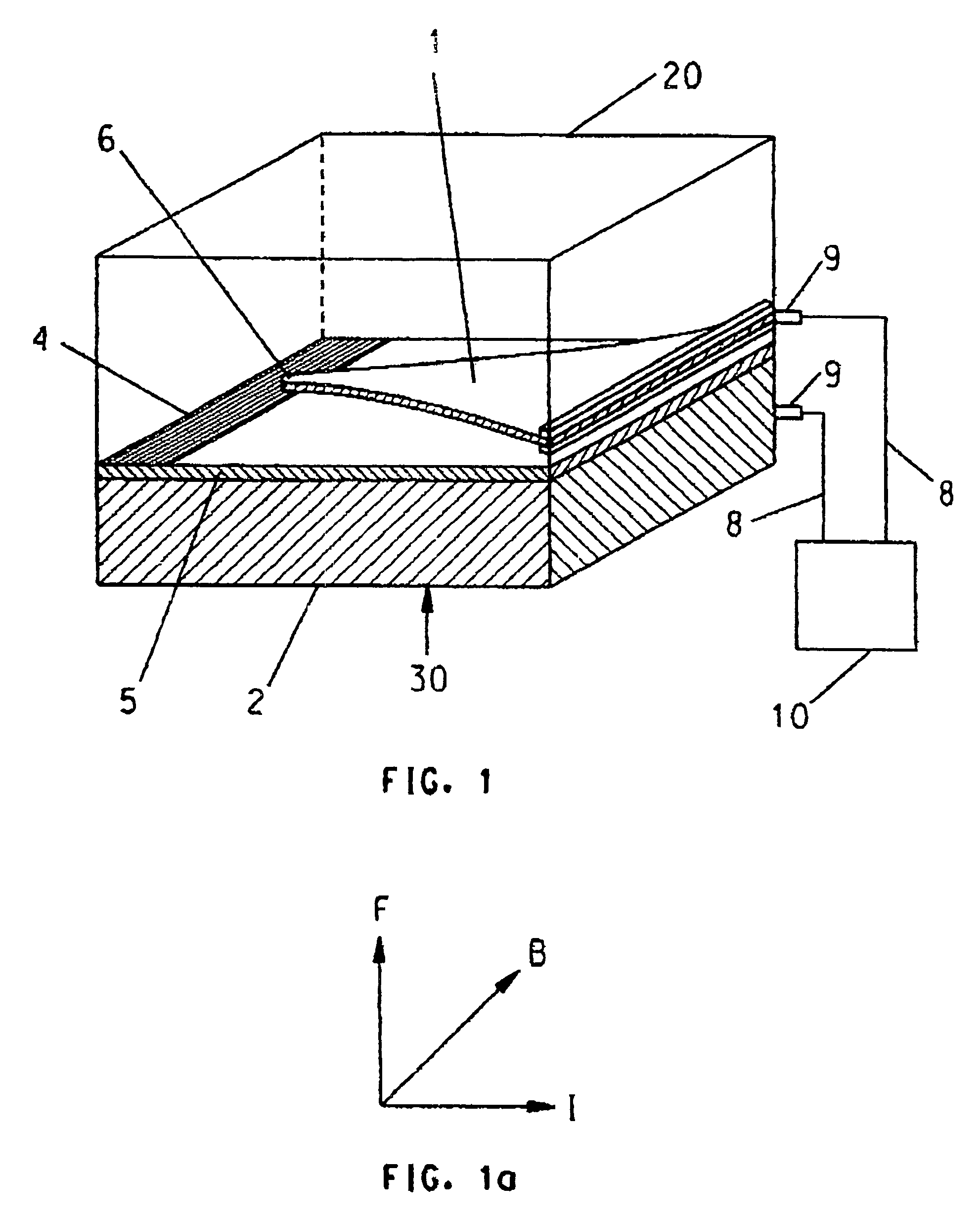
[0075]For a thermo-tunneling converter, consider the following dimensions in FIG. 1, 2 or 3:

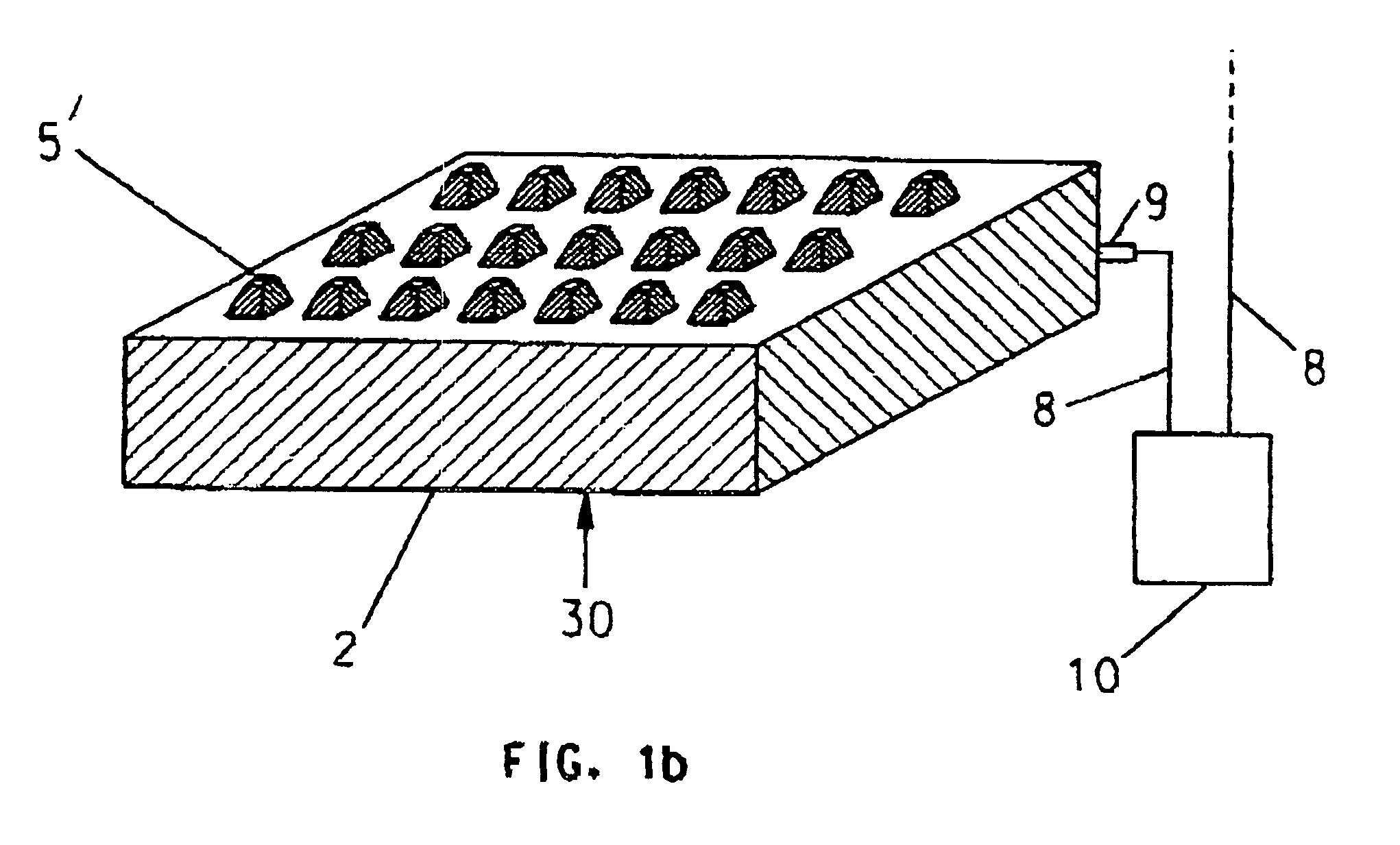
[0076]The total overlapping tunneling area Y of the facing electrodes is 1 square centimeter or 10−4 square meters. The length L of the flexible electrode 1 is 2 centimeters, and the maximum width W is 1 centimeter. The length L and width W are defined similarly for FIG. 3, but electrode 1 is wrapped around into a spiral shape as compared to a linear shape for FIG. 1. The facing surface of electrode 1 is surface-patterned or has a surface roughness such that the total tunneling area X (the sum of all x's) is one-tenth the total surface area Y or 10−5 square meters. The permanent magnet material used in electrode 2 has a field strength B of 1.2 Tesla. The voltage V between the electrodes is 0.15 volts. The permittivity constant ∈ of either vacuum or rarified inert gas between electrodes 1 and 2 is equal to 8.8×10⁻¹² farads per meter. The resistivity r of the flexible electrode 1 is assumed to ...

example 2

[0082]Another example of the versatility of this invention is in the choice of materials. The preferred embodiment, as described in Example 1, includes a metal foil as one of the electrodes. Another embodiment could use a single-crystal silicon as the flexible electrode. Although silicon is not normally regarded as a flexible material, it is routinely fabricated in the industry with a roughness of 0.5 nanometers and a flatness of 1 micrometer across a square centimeter surface. Although silicon is much stiffer than a metal foil as measured by the Young's Modulus, its flatness indicates that very little bending is required to approach ideal flatness. The forces generated by the invention will be shown to be able to bend a silicon wafer by the one micron needed flatten it completely. Overall, using silicon as the base material for the flexible or both electrodes has several advantages: (1) silicon wafers are readily available at low cost, (2) silicon wafers have desirable roughness an...


PUM


Abstract

An improved design for maintaining separation between electrodes in tunneling, diode, thermionic, and other devices is disclosed. At least one electrode is made from flexible material. A magnetic field is present to combine with the current flowing in the flexible electrode and generate a force that counterbalances the electrostatic force between the electrodes. The balancing of forces allows the separation and parallelism between the electrodes to be maintained at a very small spacing without requiring the use of multiple control systems, actuators, or other manipulating means, or spacers. The shape of one or both electrodes is designed to maintain a constant separation over the entire overlapping area of the electrodes. The end result is an electronic device that maintains two closely spaced parallel electrodes in stable equilibrium with a uniform gap therebetween over a large area in a simple configuration for simplified manufacturability and use to convert heat to electricity or electricity to cooling.

Description

BACKGROUND[0001]1. Field of the Invention[0002]The present invention pertains to diode, thermionic, tunneling, and other devices that are designed to have very small spacing between electrodes and in some cases also require thermal isolation between electrodes. The invention may be applied to thermo-tunneling generators and heat pumps, and can be applied to similar systems using thermionic and thermoelectric methods. These thermo-tunneling generators and heat pumps convert thermal energy into electrical energy and can operate in reverse to provide refrigeration. The invention may also be applied to any device that requires close, parallel spacing of two electrodes with a voltage applied and current flowing between them.[0003]2. Description of the Prior Art[0004]The phenomenon of high-energy electron flow from one conductor (emitter) to another conductor (collector) has been used in many electronic devices and for a variety of purposes. For example, vacuum-tube diodes were implemente...

Claims


Application Information

Patent Timeline
Patent Type & Authority Patents(United States)
IPC IPC(8): H02N3/00F25B21/02
CPCF03G7/00F03G6/00F03G6/092F03G7/092
Inventor MAKANSI, TAREK
Owner TEMPRONICS INC
Why Eureka
Try Eureka