

Triple gate and double gate finfets with different vertical dimension fins
- Summary
- Abstract
- Description
- Claims
- Application Information
AI Technical Summary
Benefits of technology
Problems solved by technology
Method used
Image

Examples
Embodiment Construction
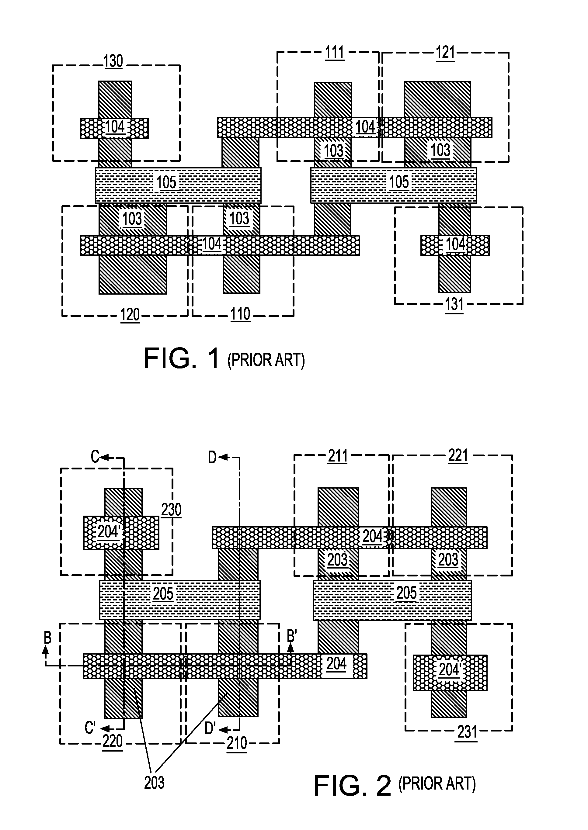
[0036]Before describing the present invention in detail, a discussion on the prior SRAM structures is provided. The discussion on the prior SRAM structures is made herein to clearly illustrate the advantages provided by the present invention over the prior art.
[0037]Referring to FIG. 1, a top-down schematic view of an exemplary six-transistor SRAM structure utilizing planar MOSFETs according to the prior art is shown. Located within the substrate (not shown explicitly) are semiconductor surfaces 103, gate electrodes 104, and a first level of metal wiring 105. These six transistors in the SRAM structure include a first pull up PFET 110, a first pull down NFET 120, a first pass gate NFET 130, a second pull up PFET 111, a second pull down NFET 121, and a second pass gate NFET 131. Noteworthy are the different widths between the semiconductor area for the first pull down NFET 120 and the corresponding semiconductor area for a first pass gate NFET 130 needed to maintain a beta ratio arou...
PUM
 Abstract
Description
Claims
Application Information