Optical disc
a technology of optical discs and optical discs, applied in the field of optical discs, can solve the problems of difficult embedding of ic memory chips and antenna coils in these films, design and manufacturing, and the possibility of restrictions on the size of elements or functions of known optical discs, so as to facilitate the design and manufacture of optical discs and improve the function of them
- Summary
- Abstract
- Description
- Claims
- Application Information
AI Technical Summary
Benefits of technology
Problems solved by technology
Method used
Image
Examples
first embodiment
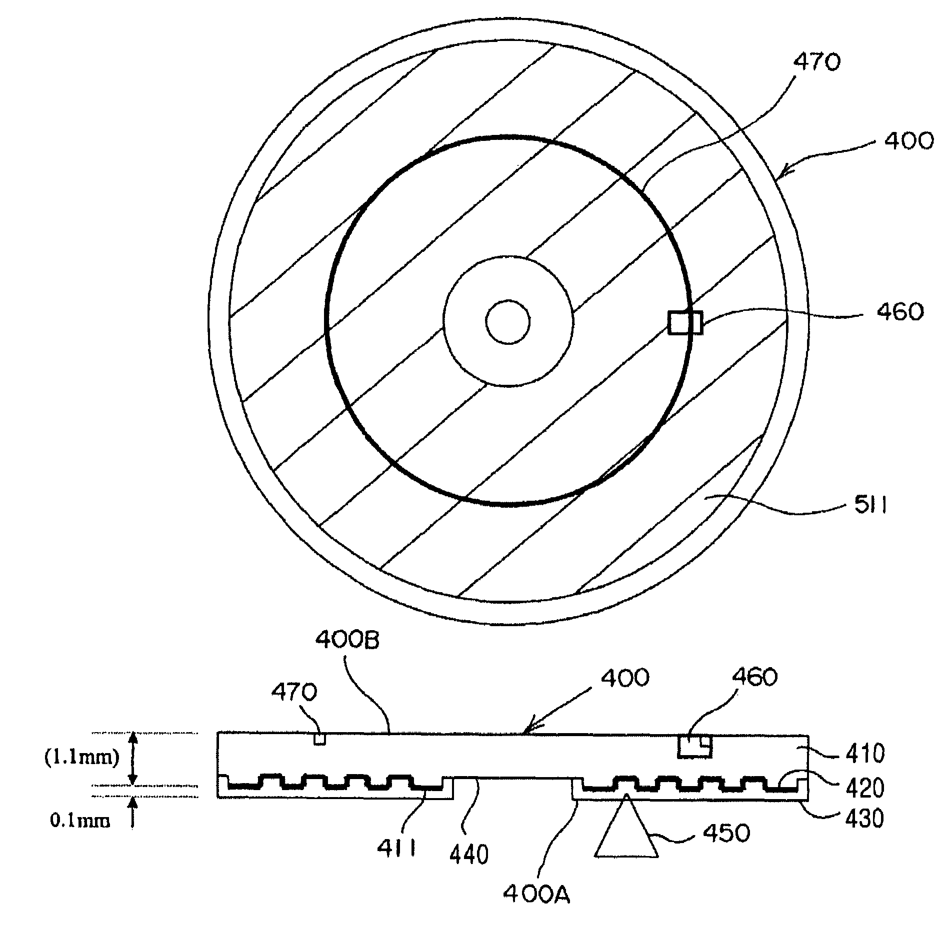
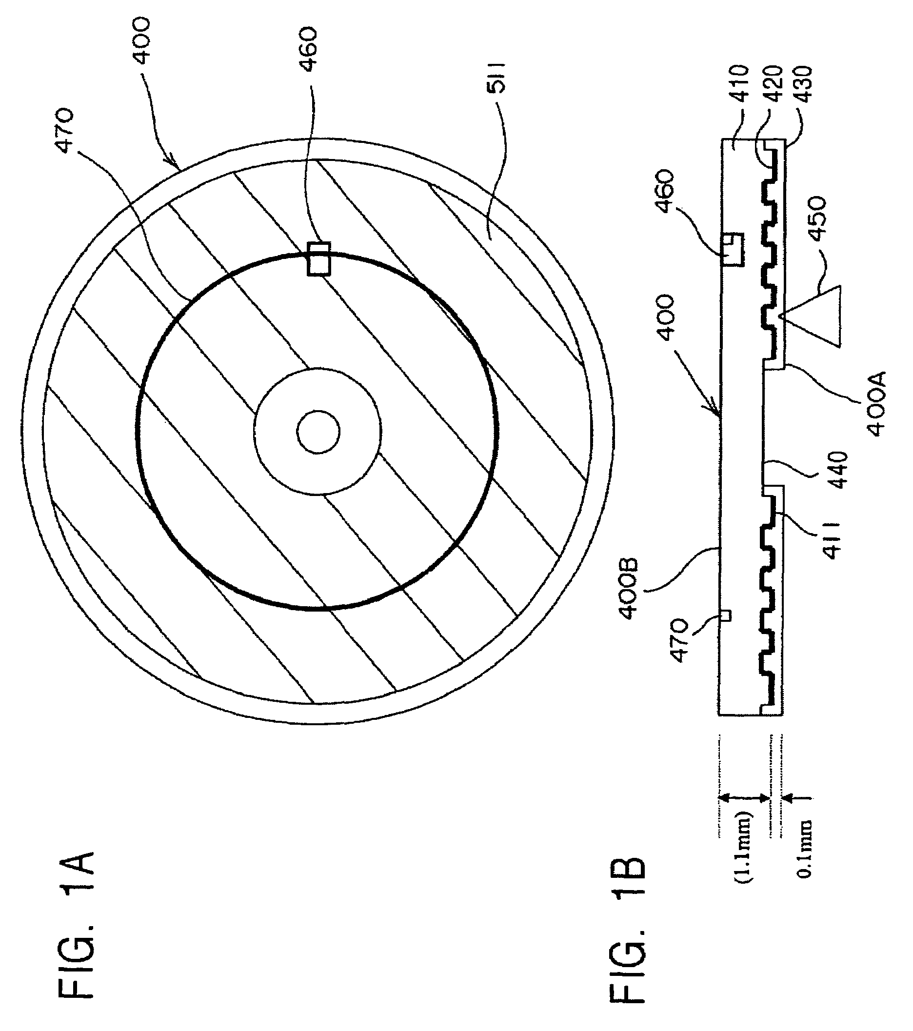
[0045]FIG. 1A is a plan view showing the structure of a Blu-ray disc (BD) having an IC memory chip and an antenna coil according to a first embodiment of the present invention. FIG. 1B is a cross-sectional view of the BD.
[0046]Referring to FIGS. 1A and 1B, a BD 400 of the first embodiment has a base 410 made of, for example, polycarbonate, a signal recording surface 411 that is a series of pits, and a reflective film 420 that is a layer made of aluminum. The signal recording surface 411 is formed on the bottom surface (first surface) of the base 410 and the reflective film 420 is formed on the signal recording surface 411. A cover layer 430 made of a transparent resin is formed on the reflective film 420.
[0047]A center portion 440 to which a disk chuck (not shown) fits is provided around the center of the BD 400. The overall thickness of the BD 400 is defined to be a value around 1.2 mm. The base 410 has a thickness of 1.1 mm and the cover layer 430 has a thickness of 0.1 mm.
[0048]T...
second embodiment
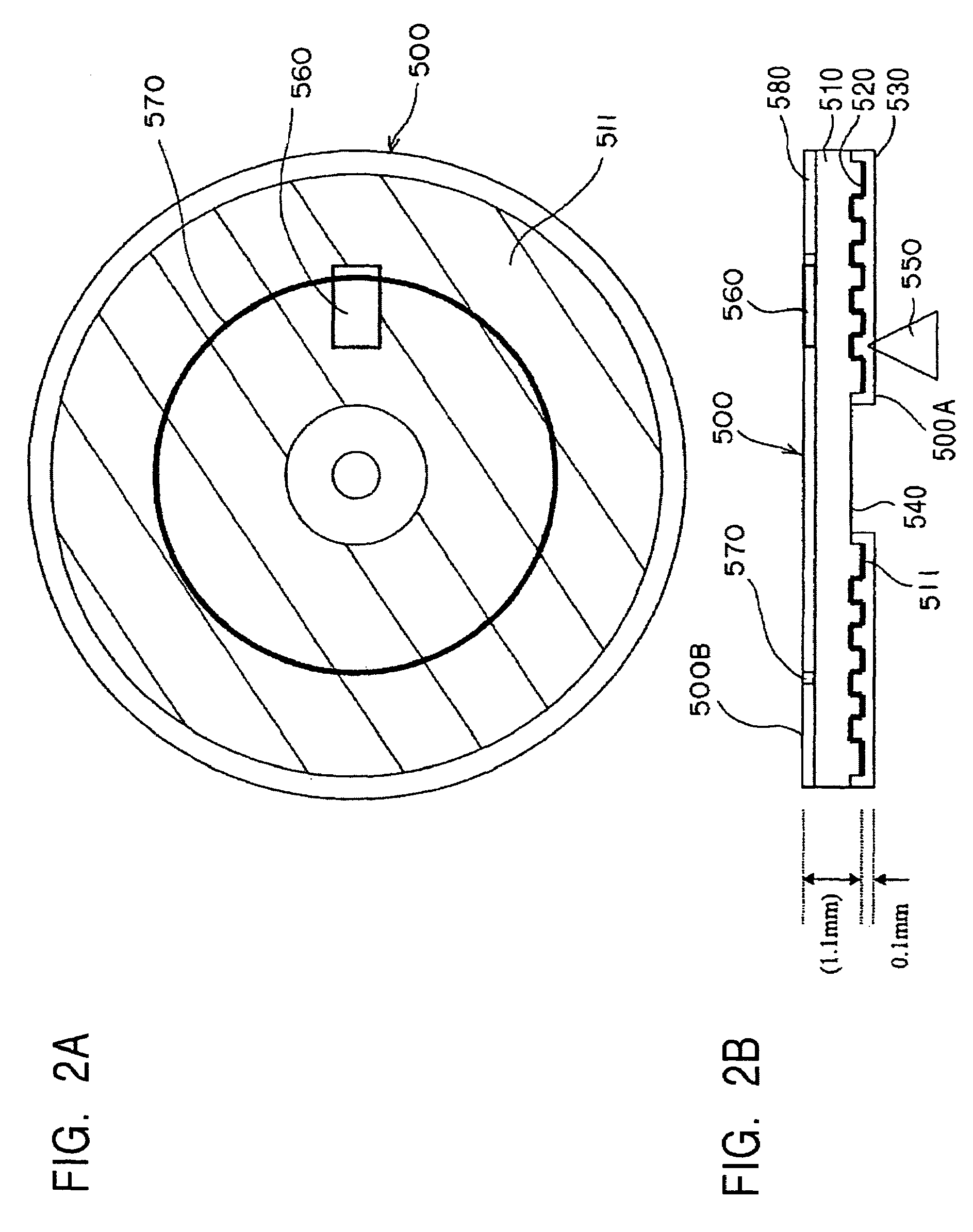
[0055]FIG. 2A is a plan view showing the structure of a BD having an IC memory chip and an antenna coil according to a second embodiment of the present invention. FIG. 2B is a cross-sectional view of the BD.
[0056]Referring to FIGS. 2A and 2B, a BD 500 of the second embodiment has a base 510, a signal recording surface 511 that is a series of pits, and a reflective film 520 made of aluminum or the like, as in FIGS. 1A and 1B. The signal recording surface 511 is formed on the bottom surface (first surface) of the base 510 and the reflective film 520 is formed on the signal recording surface 511. A cover layer 530 made of a transparent resin is formed on the reflective film 520. A center portion 540 is provided around the center of the BD 500.
[0057]The BD 500 is irradiated with a light beam 550 from the cover layer 530 side. Signals on the series of pits are read by the light reflected from the reflective film 520.
[0058]In the BD 500, a label 580 made of a resin is adhered to the top s...
third embodiment
[0063]Although both the minute IC memory chip 560 and the antenna coil 570 are provided in the label 580 in the second embodiment, one of them may be provided in the label 580 and the other one may be embedded inside the base 510. FIGS. 4A and 4B illustrate an example in which the minute IC memory chip 560 is embedded inside the base 510 and the antenna coil 570 is provided in the label 580 according to a third embodiment of the present invention. The same reference numerals are used in FIGS. 4A and 4B to identify the same components shown in FIGS. 2A and 2B. The description of such components is omitted here.
PUM
| Property | Measurement | Unit |
|---|---|---|
| thickness | aaaaa | aaaaa |
| thickness | aaaaa | aaaaa |
| thickness | aaaaa | aaaaa |
Abstract
Description
Claims
Application Information
 - R&D
- Intellectual Property
- Life Sciences
- Materials
- Tech Scout
- Unparalleled Data Quality
- Higher Quality Content
- 60% Fewer Hallucinations
Browse by: Latest US Patents, China's latest patents, Technical Efficacy Thesaurus, Application Domain, Technology Topic, Popular Technical Reports.
© 2025 PatSnap. All rights reserved.Legal|Privacy policy|Modern Slavery Act Transparency Statement|Sitemap|About US| Contact US: help@patsnap.com


