Dry etching apparatus, dry etching method, and plate and tray used therein
- Summary
- Abstract
- Description
- Claims
- Application Information
AI Technical Summary
Benefits of technology
Problems solved by technology
Method used
Image

Examples
Embodiment Construction
[0034]The following description will describe in detail embodiments of the invention with reference to the accompanying drawings.
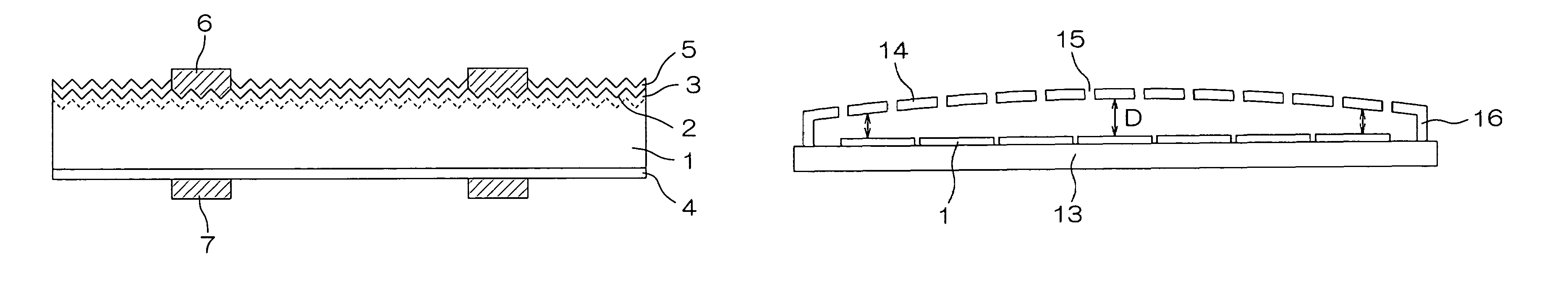
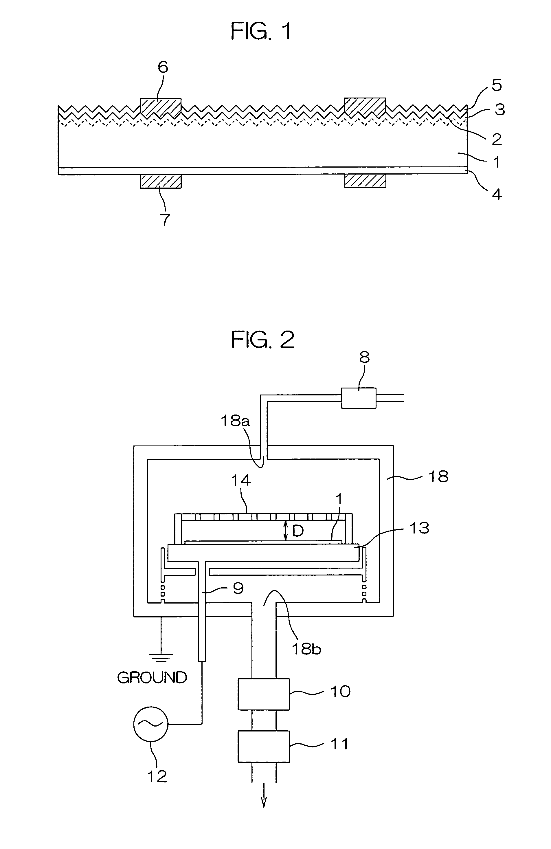
[0035]FIG. 1 is a view showing a structure of a solar cell fabricated with the use of a dry etching apparatus of the invention. Numeral 1 denotes a silicon substrate, numeral 2 denotes textures formed on the silicon substrate 1, numeral 3 denotes an impurity diffusing layer on the light-reception surface, numeral 4 denotes an impurity diffusing layer (BSF) on the back surface, numeral 5 denotes an anti-reflection layer formed on the textures 2, numeral 6 denotes a surface electrode, and numeral 7 denotes a back surface electrode.
[0036]The silicon substrate 1 is a single-crystalline or multi-crystalline silicon substrate. The substrate is of either a p-type or an n-type. The silicon substrate 1 is formed through the Czochralski method or the like in the case of single-crystalline silicon, and through casting process or the like in the case of multi-crystall...
PUM
| Property | Measurement | Unit |
|---|---|---|
| Distance | aaaaa | aaaaa |
Abstract
Description
Claims
Application Information
 - R&D Engineer
- R&D Manager
- IP Professional
- Industry Leading Data Capabilities
- Powerful AI technology
- Patent DNA Extraction
Browse by: Latest US Patents, China's latest patents, Technical Efficacy Thesaurus, Application Domain, Technology Topic.
© 2024 PatSnap. All rights reserved.Legal|Privacy policy|Modern Slavery Act Transparency Statement|Sitemap