
Light emitting chip package and light source module

a technology of light emitting chip and light source module, which is applied in the direction of electrical apparatus, semiconductor devices, semiconductor/solid-state device details, etc., can solve the problems of increasing the need to dissipate heat, affecting the brightness and life of light emitting diodes, and generating a large amount of hea

Inactive Publication Date: 2008-12-02
CHIPMOS TECH INC
View PDF4 Cites 2 Cited by
  • Summary
  • Abstract
  • Description
  • Claims
  • Application Information

AI Technical Summary

Benefits of technology

[0008]The present invention is directed to a light source module with longer life time.
[0009]The present invention is directed to a light emitting package chip with high thermal dissipation efficiency.
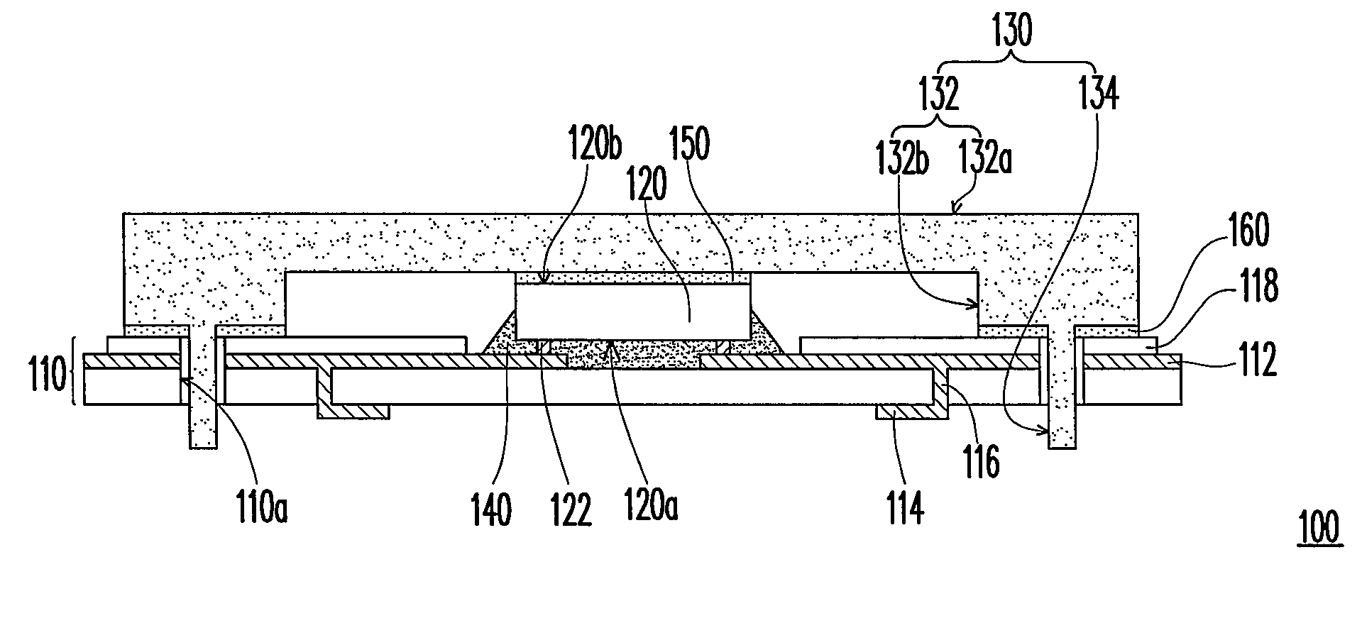
[0030]In view of the above, according to the present invention, the protrusions of the thermal enhanced cover are inserted through the through holes of the carrier. Hence, the heat generated by the light emitting chip can be conducted to the other surface of the carrier through the thermal enhanced cover to enhance the thermal dissipation efficiency. Further, each protrusion of the thermal enhanced cover in the light emitting chip package is further connected to a trench in a metal substrate. Hence, the heat generated by the light emitting chip can be conducted to the metal substrate through the thermal enhanced cover to enhance the thermal dissipation efficiency.

Problems solved by technology

Nevertheless, light emitting diodes generate a large amount of heat during operation and the brightness and life time of the light emitting diodes are affected by temperature.
Therefore, as the power of light emitting diodes increases, the need to dissipate heat increases.
However, utilizing a complex heat dissipation system will result in an oversized device and an increase in the manufacturing costs.

Method used


Image

  • Light emitting chip package and light source module
  • Light emitting chip package and light source module
  • Light emitting chip package and light source module

Examples


Embodiment Construction

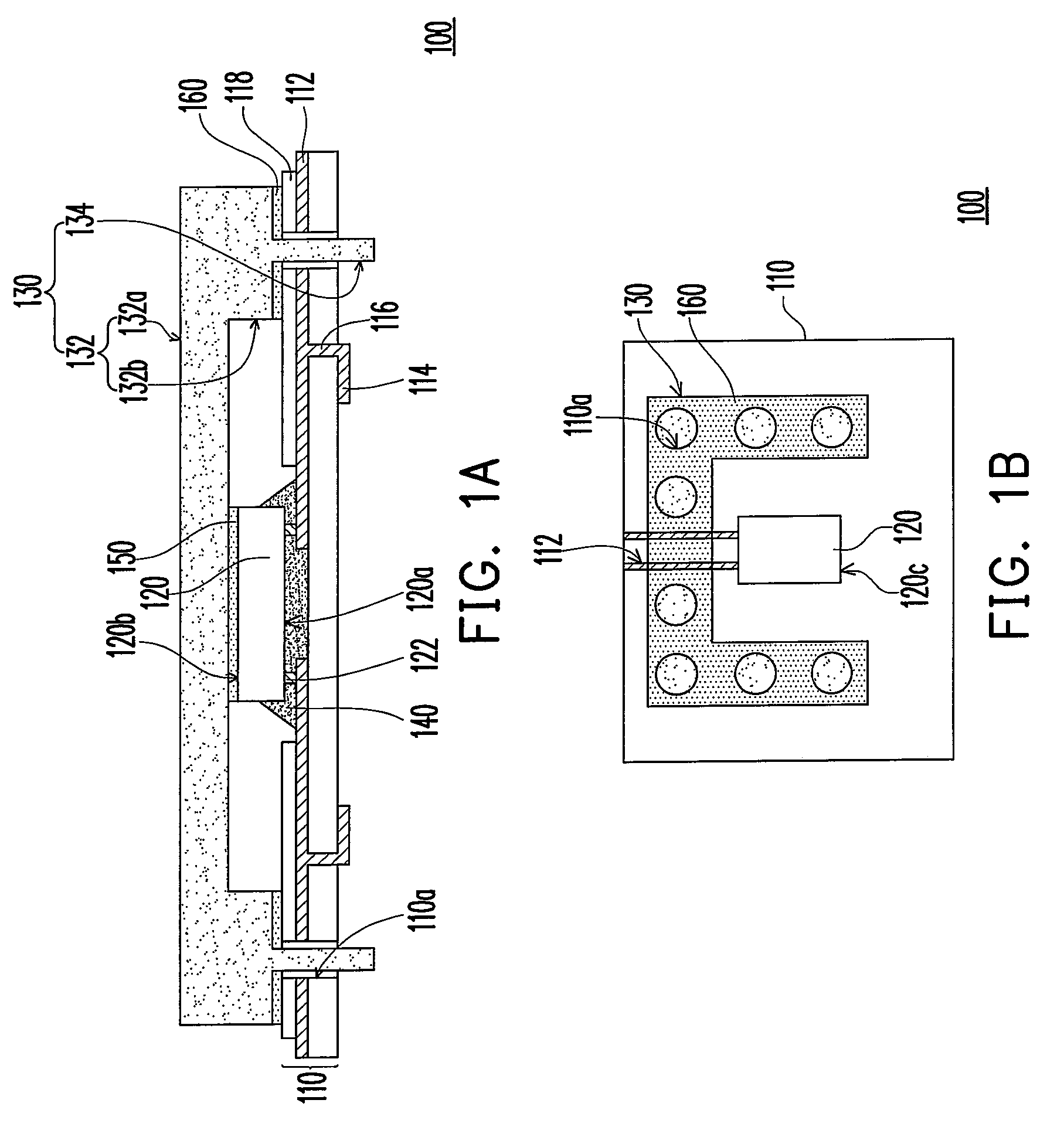
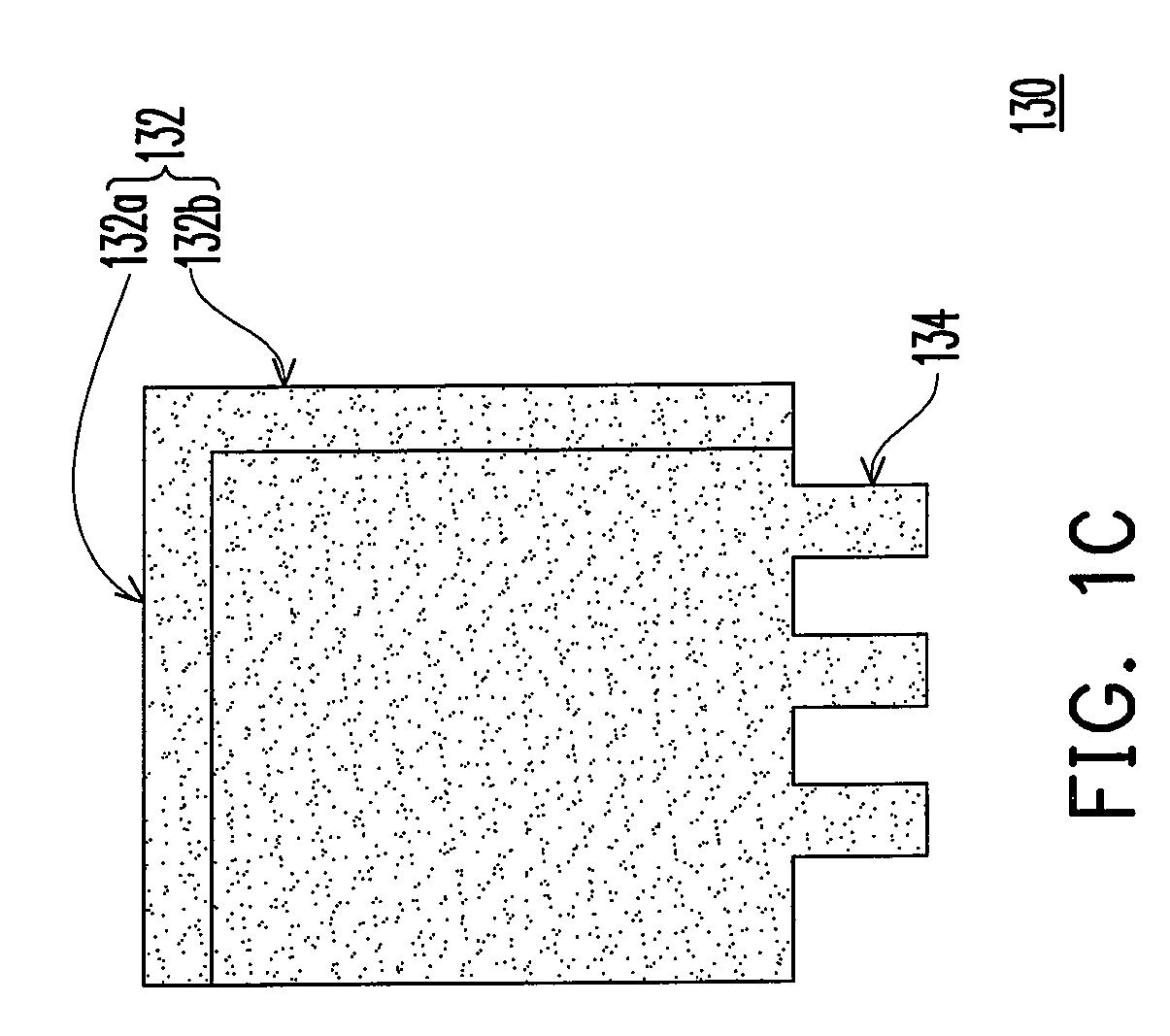
[0037]FIG. 1A is a schematic cross-sectional view illustrating a light emitting chip package according to one embodiment of the present invention and FIG. 1B is a schematic top view illustrating the light emitting chip package of FIG. 1A with some components omitted. FIG. 1C is a schematic cross-sectional view illustrating the thermal enhanced cover of the light emitting chip package of FIG. 1A. Please refer to FIG. 1A and FIG. 1B. In the present embodiment, a light emitting chip package 100 includes a carrier 110, at least one light emitting chip 120 and a thermal enhanced cover 130. Herein, the carrier 110 includes a plurality of through holes 110a and the light emitting chip 120 is disposed on the carrier 110. The light emitting chip 120 has an active surface 120a, a back surface 120b opposite the active surface 120a, and a plurality of bumps 122. The bumps 122 are disposed on the active surface 120a of the light emitting chip 120. Further, the light emitting chip 120 is electric...


PUM


Abstract

A light emitting chip package having a carrier, at least one light emitting chip and a thermal enhanced cover is provided. The carrier includes a plurality of through holes. The light emitting chip is disposed on the carrier. The light emitting chip has an active surface, a back surface opposite to the active surface and a plurality of bumps disposed on the active surface. The light emitting chip is electrically connected to the carrier through the bumps. The thermal enhanced cover is disposed on the carrier to expose at least one side of the light emitting chip. The thermal enhanced cover includes a cover body and a plurality of protrusions connected thereto. A portion of the cover body is above the back surface of the light emitting chip. The protrusions are respectively inserted through the through holes. Therefore, the thermal dissipation efficiency of the light emitting chip package is improved.

Description

CROSS-REFERENCE TO RELATED APPLICATION[0001]This application claims the priority benefit of Taiwan application serial. no. 95145368,filed Dec. 6, 2006. All disclosure of the Taiwan application is incorporated herein by reference.BACKGROUND OF THE INVENTION[0002]1. Field of the Invention[0003]The present invention relates to a light source module and a chip package, and more particularly, the present invention relates to a backlight module and a light emitting chip package.[0004]2. Description of Related Art[0005]Recently, light emitting diode (LED) devices that use semiconductors containing gallium nitride compounds such as GaN, AlGaN, InGaN are gaining popularity. The Group III nitride is a material with wide band gap and its light wavelength ranges from ultraviolet light to red light. In other words, the range covers almost the entire visible light spectrum. Further, in comparison to conventional light bulbs, light emitting diodes are characterized as compact, long lasting, driven...

Claims


Application Information

Patent Timeline
Patent Type & Authority Patents(United States)
IPC IPC(8): H01L33/00H01L33/48H01L33/64
CPCH01L33/483H01L33/64H01L51/529H01L2224/16225H01L2224/73204H01L2224/73253H01L2924/12044H01L2924/00014H01L2924/00011H10K50/87H01L2924/00H01L2224/0401
Inventor LIU, MEN-SHEWPAN, YU-TANG
Owner CHIPMOS TECH INC
Learn More