Organic electroluminescent element

a technology of electroluminescent elements and organic materials, which is applied in the direction of organic chemistry, luminescent compositions, semiconductor devices, etc., can solve the problems of unreachable high-efficiency light emission, and achieve high luminous efficiency, long life, and low driving voltage

Inactive Publication Date: 2017-09-14
NIPPON STEEL CHEMICAL CO LTD
View PDF19 Cites 252 Cited by
  • Summary
  • Abstract
  • Description
  • Claims
  • Application Information

AI Technical Summary

Benefits of technology

[0026]A light-emitting layer of the organic EL device of the present invention is obtained by mixing a plurality of host materials formed of a combination of specific host mater...

Problems solved by technology

Then, investigations have been made on using a europium complex as an attempt to use a triplet excited state, but highly efficient light emission has not been accomplish...

Method used


Image

  • Organic electroluminescent element
  • Organic electroluminescent element
  • Organic electroluminescent element

Examples


example 1

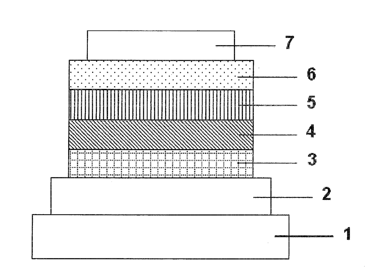
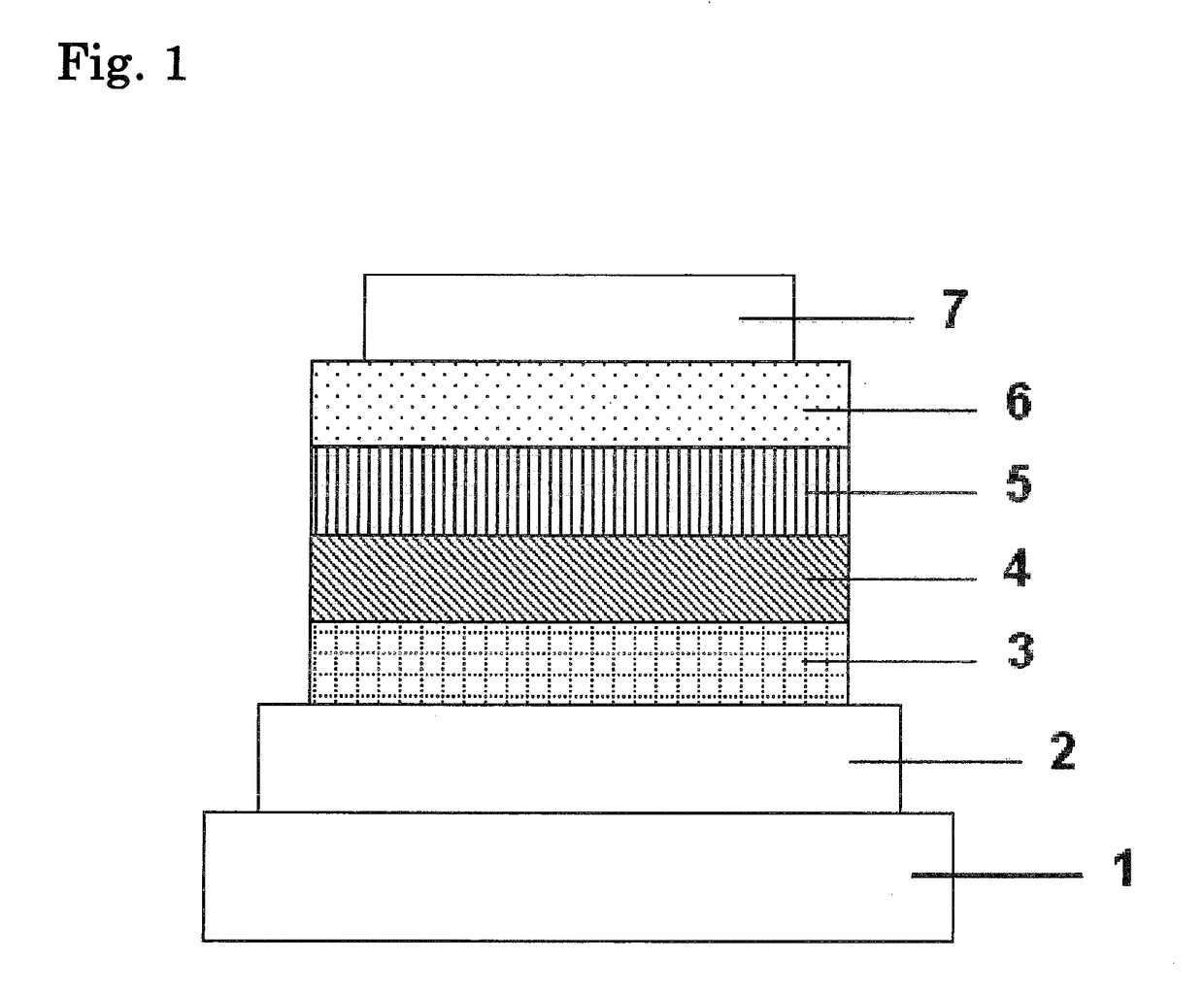
[0099]Each thin film was laminated on a glass substrate having formed thereon an anode formed of ITO having a thickness of 110 nm by a vacuum deposition method at a degree of vacuum of 4.0×10⁻⁵ Pa. First, CuPc serving as a hole-injecting layer was formed on ITO so as to have a thickness of 20 nm, and then NPB serving as a hole-transporting layer was formed so as to have a thickness of 20 nm. Next, the preliminarily mixed host H1 serving as a host for a light-emitting layer and Ir(PPy)3 serving as a light-emitting dopant were co-deposited from different deposition sources to form a light-emitting layer having a thickness of 30 nm. At this time, a deposition rate ratio between the H1 and Ir(PPy)3 was 94:6. Next, BAlq serving as a hole-blocking layer was formed so as to have a thickness of 10 nm, and then Alq3 serving as an electron-transporting layer was formed so as to have a thickness of 40 nm. Further, lithium fluoride (LiF) serving as an electron-injecting layer was formed on the ...

example 2

[0101]An organic EL device was produced in the same manner as in Example 1 except that in Example 1, the H2 was used as a host for a light-emitting layer. An external power source was connected to the resultant organic EL device to apply a DC voltage to the device. As a result, an emission spectrum having a local maximum wavelength of 517 nm was observed, and hence it was found that light emission from Ir(PPy)3 was obtained. The luminance, driving voltage, luminous efficiency, and luminance half-life of the produced organic EL device are shown in Table 2.

examples 3 to 5

[0107]Organic EL devices were continuously produced three times in the same manner as in Example 1. The device produced in the first time was defined as Example 3, the device produced in the second time was defined as Example 4, and the device produced in the third time was defined as Example 5. The luminance, driving voltage, and luminous efficiency of each of the produced organic EL devices are shown in Table 3. The luminance, the driving voltage, and the luminous efficiency are values at a driving current of 20 mA / cm2, and are initial characteristics.


PUM


Abstract

Provided is a homogeneous organic EL device having a low driving voltage, high luminous efficiency, and a long lifetime. The device is an organic electroluminescent device including a light-emitting layer between an anode and a cathode opposite to each other, in which: the light-emitting layer contains a host material and a light-emitting dopant material; the host material is a material obtained by preliminarily mixing two or more kinds of compounds selected from compounds each having a structure in which two nitrogen atoms of an indolocarbazole ring are each substituted with an aromatic hydrocarbon group or an aromatic heterocyclic group; and the light-emitting layer is formed by co-depositing the preliminarily mixed host material and the light-emitting dopant material in a vacuum.

Description

TECHNICAL FIELD[0001]The present invention relates to an organic electroluminescent device (referred to as “organic EL device”).BACKGROUND ART[0002]In general, the simplest structure of an organic EL device includes a light-emitting layer and a pair of opposing electrodes between which the layer is interposed. That is, in the organic EL device, when an electric field is applied between both the electrodes, an electron is injected from a cathode and a hole is injected from an anode. The device utilizes a phenomenon in which energy produced at the time of the recombination of the electron and the hole in the light-emitting layer is emitted as light.[0003]In recent years, progress has been made in developing an organic EL device using an organic thin film. In particular, development has been made in order to enhance luminous efficiency. In the development, the efficiency of injection of carriers from electrodes has been improved through optimization of the kind of the electrodes. In ad...

Claims


Application Information

Patent Timeline
IPC IPC(8): H01L51/00C09K11/06C07D487/04C09K11/02
CPCH01L51/0072C09K11/025C09K11/06C07D487/04H01L51/0067H01L51/5012C09K2211/185H01L51/001H01L51/504H01L2251/5384H01L51/5016H01L51/0085H05B33/10H10K85/654H10K85/6572H10K50/11H10K2101/10H10K2101/90H10K2101/20H05B33/14H10K85/341H10K50/12H10K85/342H10K50/13H10K71/164
Inventor TADA, MASASHIKAI, TAKAHIROHOTTA, MASANORIOGAWA, JUNYASAKAI, MITSURUIKENAGA, YUJIUEDA, TOKIKONOGUCHI, KATSUHIDE
Owner NIPPON STEEL CHEMICAL CO LTD
Why Eureka
Try Eureka