Formation of circuitry with modification of feature height

a technology of feature height and circuitry, applied in the direction of semiconductor devices, semiconductor/solid-state device details, electrical devices, etc., can solve the problems of reducing the projection distance, affecting the quality of circuitry, so as to reduce the projection distance

Active Publication Date: 2008-12-09
TESSERA INC
View PDF67 Cites 87 Cited by
  • Summary
  • Abstract
  • Description
  • Claims
  • Application Information

AI Technical Summary

Benefits of technology

[0017]According to another aspect of the invention, a method is provided for treating a starting unit. The starting unit includes a dielectric layer having an inside surface and an outside surface, one or more electrically-conductive elements extending on the dielectric layer remote from the outside surface, and a plurality of posts extending from the one or more conductive elements through the dielectric layer and projecting beyond the outside surface by projection distances. Such method includes a step of reducing the projection distances of at least some of the posts.

Problems solved by technology

The components made by this process suffer from certain drawbacks for use as connection components in certain types of semiconductor chip packages.
While this problem can be overcome by forming additional openings in the dielectric element in alignment with the traces, this adds cost and complexity to the manufacturing process.
However, where a packaged chip is to be mounted using conventional large solder balls, this substantial height may be undesirable.

Method used


Image

  • Formation of circuitry with modification of feature height
  • Formation of circuitry with modification of feature height
  • Formation of circuitry with modification of feature height

Examples


Embodiment Construction

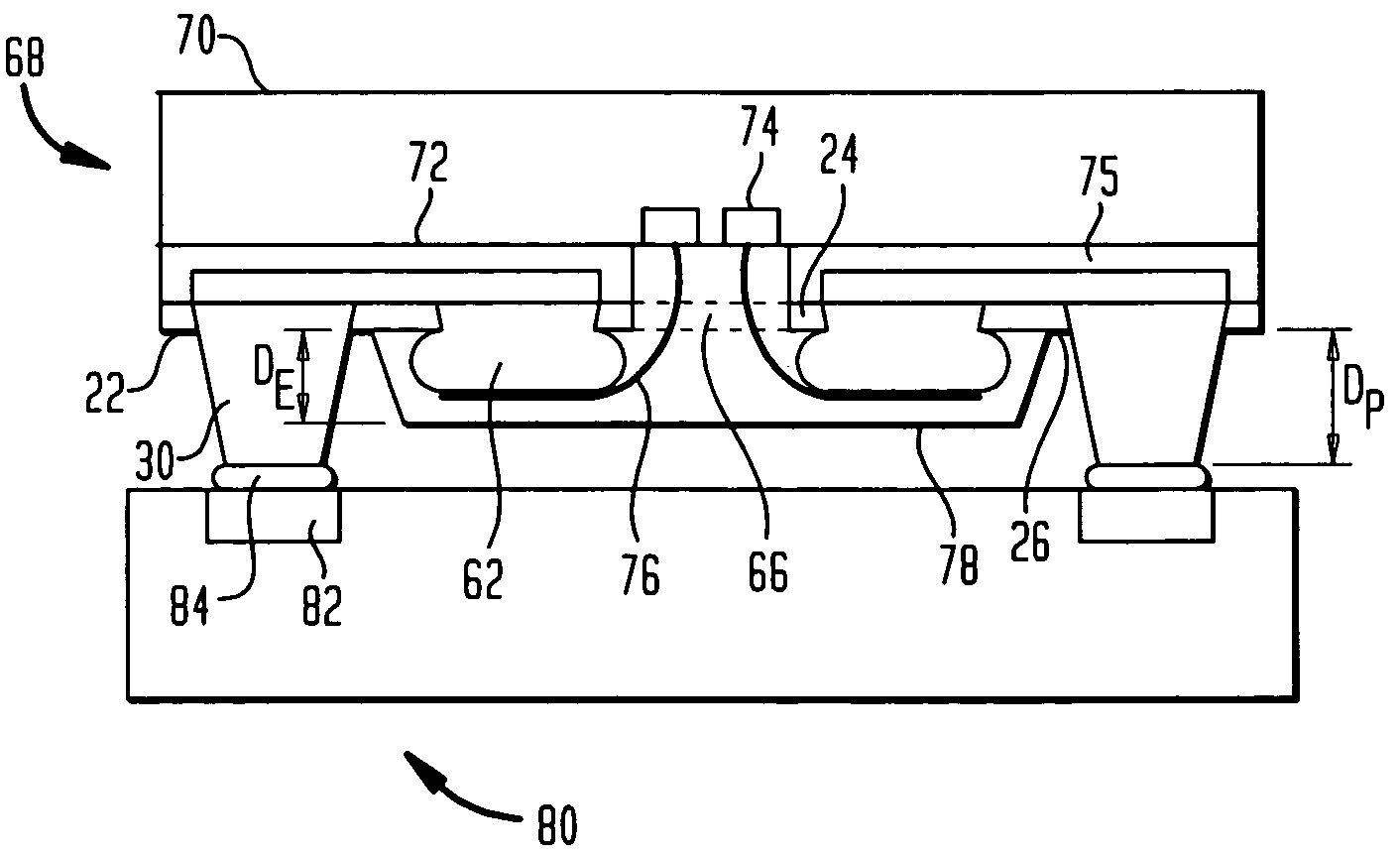
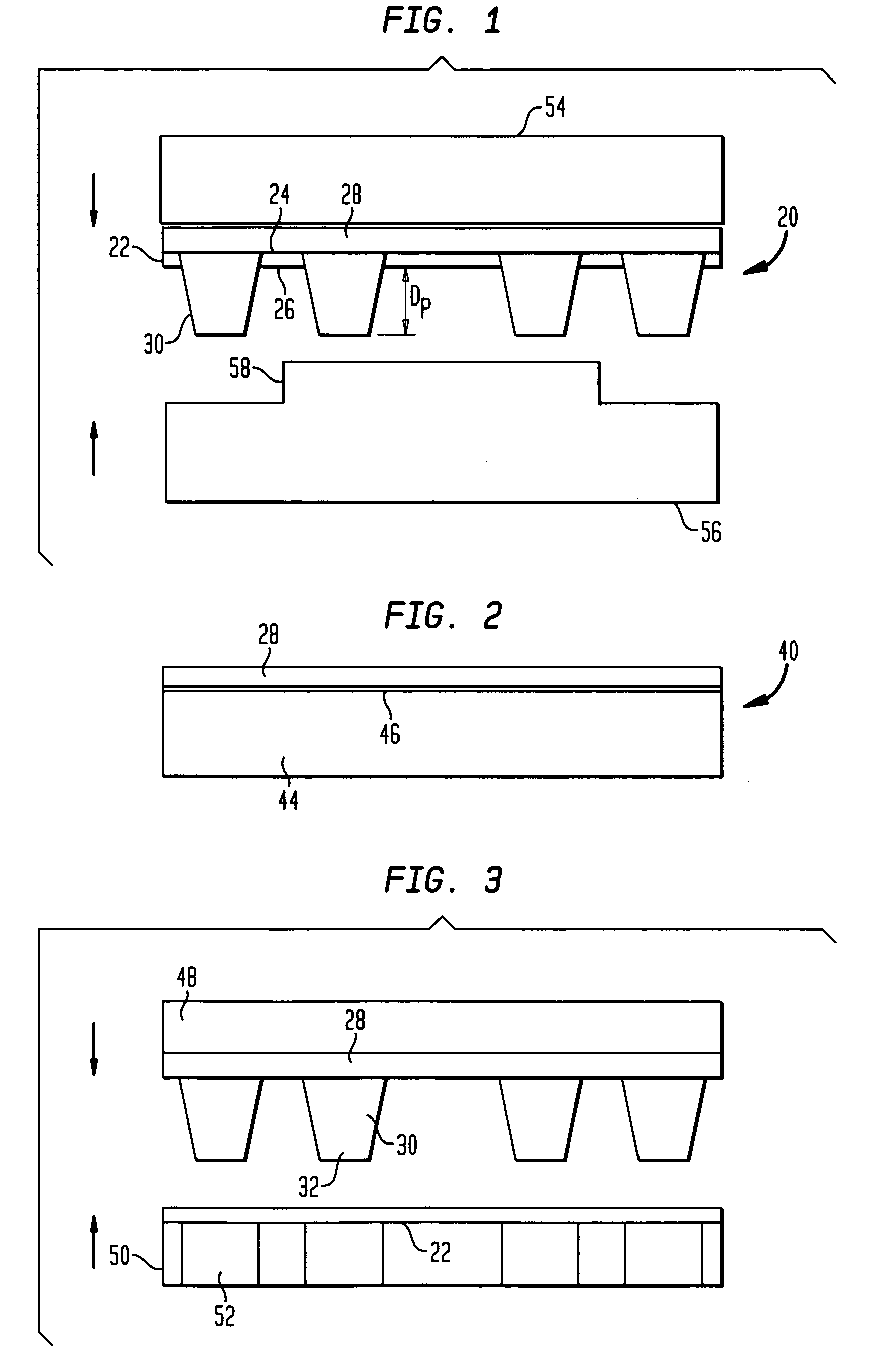
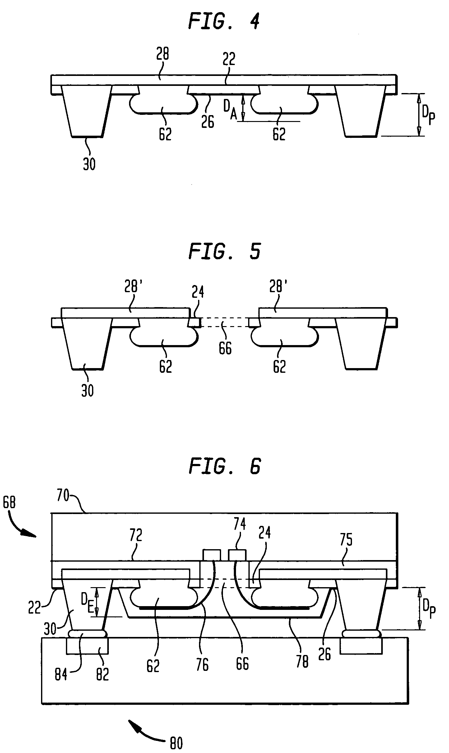
[0033]A method of fabricating a component in accordance with one embodiment of the invention utilizes a starting unit which incorporates a dielectric layer 22 (FIG. 1) having an inside surface 24 facing upwardly and an outside surface 26 facing downwardly. As used in this disclosure, terms such as “upwardly,”“downwardly,”“vertically” and “horizontally” should be understood as referring to the frame of reference of the element specified and need not conform to the normal gravitation frame of reference. The starting unit 20 also includes an electrically-conductive element 28 which, in this instance, is a unitary, generally planar metallic layer disposed on the dielectric remote from the outside surface 26. As used in this disclosure, when a conductive element is said to be “on” a dielectric element or layer, the conductive element need not be disposed on a surface of the dielectric, but instead, may be disposed within the dielectric. That is, the word “on” does not imply location at a...


PUM

PropertyMeasurementUnit
pad projection distancesaaaaaaaaaa
heightaaaaaaaaaa

Abstract

A connection component for mounting a chip or other microelectronic element is formed from a starting unit including posts projecting from a dielectric element by crushing or otherwise reducing the height of at least some of the posts.

Description

CROSS-REFERENCE TO RELATED APPLICATIONS[0001]This application claims the benefit of the filing dates of U.S. Provisional Patent Application Nos. 60 / 533,210, 60 / 533,393, and 60 / 533,437, all of which were filed Dec. 30, 2003, and 60 / 508,970 filed Oct. 6, 2003. The disclosures of all the aforesaid applications are hereby incorporated herein by reference.BACKGROUND OF THE INVENTION[0002]The present invention relates to components and assemblies useful in microelectronic assemblies, to assemblies incorporating such components and to methods of making such components and assemblies.[0003]Microelectronic elements such as semiconductor chips typically are provided in packages that protect the semiconductor chip itself from the external environment and which facilitate mounting the chip on a circuit board. For example, some microelectronic packages include a connection component incorporating a dielectric element such as a board or sheet having top and bottom surfaces and having electrically...

Claims


Application Information

Patent Timeline
Patent Type & Authority Patents(United States)
IPC IPC(8): H01L23/48H01L23/13H01L23/498
CPCH01L23/13H01L24/48H01L23/49811H01L24/49H01L24/45H01L2224/45144H01L2224/48091H01L2224/48095H01L2224/4824H01L2224/48465H01L2224/48599H01L2224/49175H01L2924/01005H01L2924/01006H01L2924/01028H01L2924/01029H01L2924/01078H01L2924/01079H01L2924/014H01L2924/14H01L2924/15311H01L2924/01033Y10T29/49208H01L2924/00014H01L2924/00H01L2224/0233H01L2224/02377H01L2224/85207H01L2224/85444H01L2224/85455H01L2924/12042
Inventor HABA, BELGACEMBEROZ, MASUDKIM, YOUNG-GONTUCKERMAN, DAVID B.
Owner TESSERA INC
Why Eureka
Try Eureka