Method of manufacturing shielded electronic circuit units

a technology of electronic circuit unit and shielding layer, which is applied in the direction of printed circuit aspect, cross-talk/noise/interference reduction, printed circuit incorporation, etc., can solve the problems of insufficient electrical shield effect through metallic film b>56/b>

Inactive Publication Date: 2009-01-20
ALPS ALPINE CO LTD
View PDF5 Cites 108 Cited by
  • Summary
  • Abstract
  • Description
  • Claims
  • Application Information

AI Technical Summary

Benefits of technology

[0014]The present invention has been finalized in view of the drawbacks inherent in the electronic circuit unit according to the related art, and it is an object of the present invention to provide an electronic circuit unit which is capable of achieving a super electrical shielding effect and sure connection between a metallic film and a grounding pattern, and a method of manufacturing the same.

Problems solved by technology

As a result, an electrical shield effect through the metallic film 56 is insufficient.
As a result, the electrical shield effect through the metallic film 56 is insufficient.

Method used


Image

  • Method of manufacturing shielded electronic circuit units
  • Method of manufacturing shielded electronic circuit units
  • Method of manufacturing shielded electronic circuit units

Examples


first embodiment

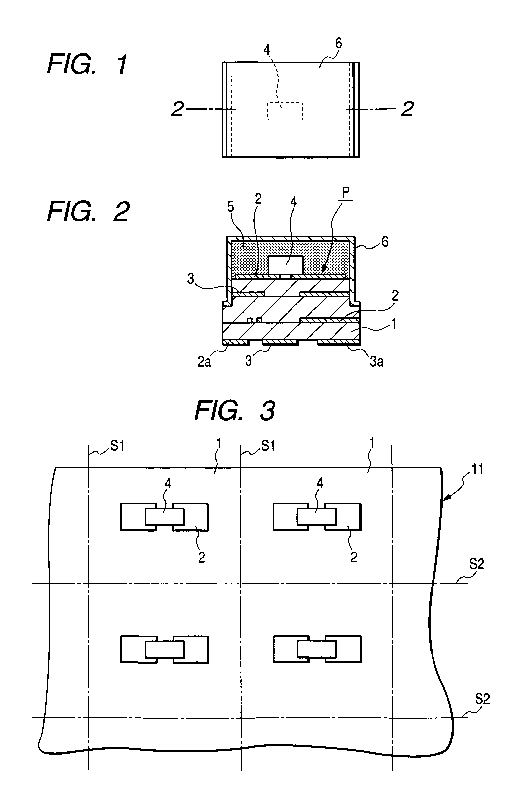
[0068]Next, a structure of an electronic circuit unit according to the invention will be described with reference to FIGS. 1 and 2. A multi-layered substrate 1 is made of an insulating material, such as a ceramic material or the like. This multi-layered substrate 1 is formed of a rectangular laminated substrate. Here, reference numeral is omitted, but the multi-layered substrate 1 has a top surface, a bottom surface, two pairs of side surfaces that are opposite to each other, and laminated layers (inner laminated layers).

[0069]A wiring pattern P has signal patterns 2 and grounding patterns 3. The signal patterns 2 of the wiring pattern P are provided on the top surface and the laminated layers (inner laminated layers) of the multi-layered substrate 1 and have a plurality of terminals 2a that are provided on the bottom surface of the multi-layered substrate 1. Further, the grounding patterns 3 are provided on the laminated layers (inner laminated layers) and the bottom surface of the...

second embodiment

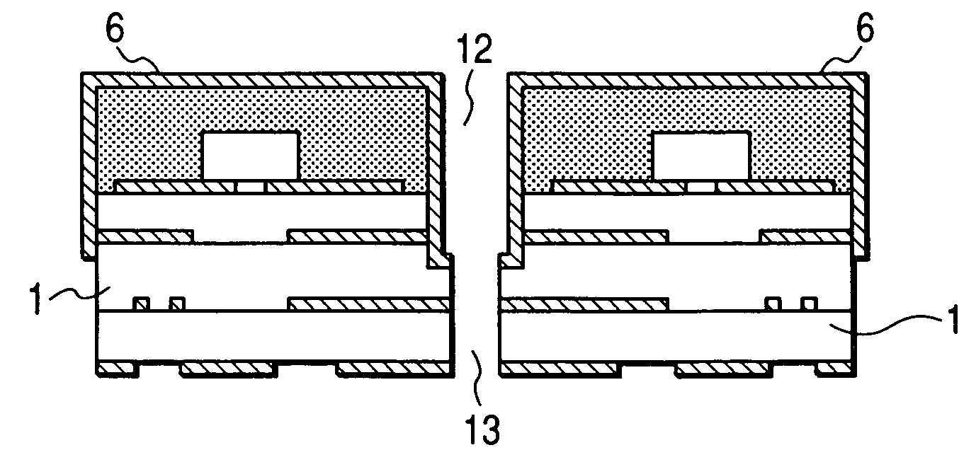
[0089]In addition, in the second embodiment, the grounding patterns 3 are exposed to each of the two pairs of side surfaces of the multi-layered substrate 1. However, the grounding patterns 3 may be exposed to one side surface of the multi-layered substrate 1 or the pair of side surfaces of the multi-layered substrate 1 that are opposite to each other.

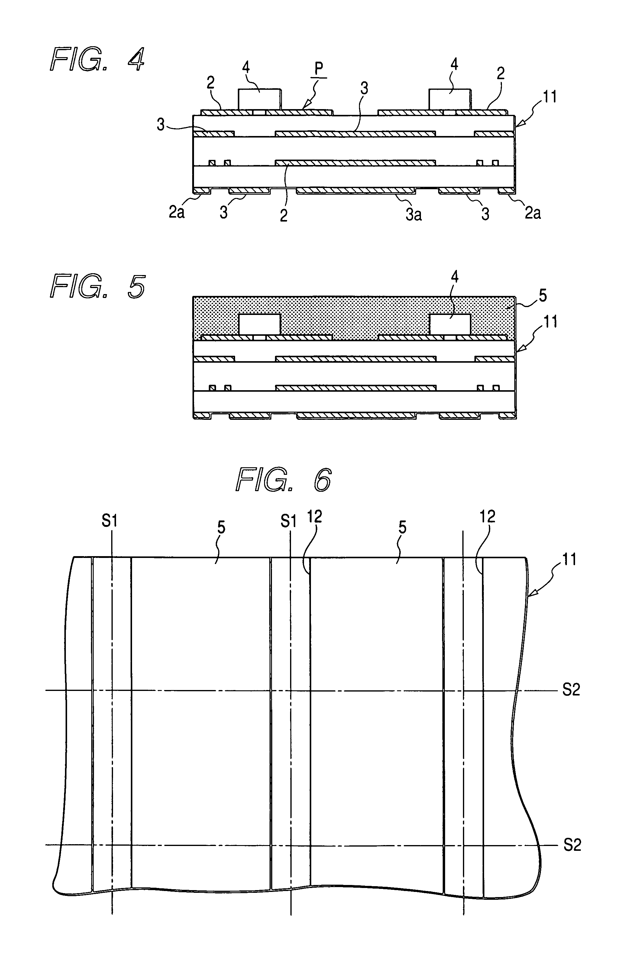
[0090]Next, a method of manufacturing the electronic circuit unit according to the second embodiment of the invention will be described with reference to FIG. 13, and FIGS. 3 to 9, which illustrate the method of manufacturing the electronic circuit unit according to the first embodiment of the invention. First, as shown in FIGS. 3 and 4, an assembly substrate 11 is prepared so as to form a plurality of multi-layered substrates 1. Then, in a first process illustrated in FIGS. 3 and 4, in the assembly substrate 11, electronic components 4 are mounted (installed) so as to correspond to each of the plurality of multi-layered substrates 1. ...

third embodiment

[0102]Next, a method of manufacturing the electronic circuit unit according to the invention will be described with reference to FIGS. 16 to 24. First, as shown in FIGS. 16 and 17, the assembly substrate 11 has cutting grooves 11b that are provided between adjacent multi-layered substrates 1 (a cutting line S1) so as to expose the grounding patterns 3 located on the laminated layers. This assembly substrate 11 is prepared so as to form the plurality of multi-layered substrates 1. Then, in a first process illustrated in FIGS. 16 and 17, in the assembly substrate 11, electronic components 4 are mounted (installed) so as to correspond to the plurality of multi-layered substrates 1.

[0103]Then, in a second process illustrated in FIGS. 18 and 19, conductor portions 14 made of conductive materials are filled into the cutting grooves 11b, and the conductor portions 14 are connected to the grounding patterns 3.

[0104]The conductor portions 14 are provided so as to be parallel to each other, a...


PUM

PropertyMeasurementUnit
widthaaaaaaaaaa
metallicaaaaaaaaaa
conductiveaaaaaaaaaa

Abstract

A metallic film and a grounding pattern are surely connected to each other so as to achieve electrical shield of an electronic circuit unit. In an electronic circuit unit, the metallic film is provided on a top surface of a sealing resin portion for burying an electronic component, the side surfaces of the sealing resin portion that are opposite to each other, and the side surfaces of the multi-layered substrate that are opposite to each other. The metallic film is connected to the grounding patterns that are provided on the top surface of the multi-layered substrate or between the laminated layers of the multi-layered substrate. Therefore, it is possible to achieve a superior electrical shielding effect through the metallic film, as compared with the related art. Since the metallic film is formed on the side surfaces of the sealing resin and the side surfaces of the multi-layered substrate, when the metallic film is formed by a plating method, the blind hole may not be provided in the related art. Therefore, it is possible to achieve the superior circulation of the plating liquid, which results in sure connection between the sure connection between the grounding pattern and the metallic film.

Description

BACKGROUND OF THE INVENTION[0001]1. Field of the Invention[0002]The present invention relates to a shielded electronic circuit unit that is suitable for a voltage controller or the like and a method of manufacturing the same.[0003]2. Description of the Related Art[0004]FIG. 36 is a cross-sectional view illustrating a main portion of an electronic circuit unit according to the related art, and FIG. 37 is a cross-sectional view of a main portion illustrating a method of manufacturing the electronic circuit unit according to the related art. Next, a structure of the electronic circuit unit according to the related art will be described with reference to FIG. 36. In a multi-layered substrate 51, a wiring pattern P1, which has signal patterns 52 and grounding patterns 53, is provided. The signal patterns 52 of the wiring pattern P1 are provided on a top surface and laminated layers (inner laminated layers) of the multi-layered substrate 51, and have terminal portions 52a that are provide...

Claims


Application Information

Patent Timeline
Patent Type & Authority Patents(United States)
IPC IPC(8): H05K3/30
CPCH01L21/561H01L23/3121H01L23/552H01L24/97H05K1/0218H01L23/29Y10T29/49146H01L2924/01015H01L2924/01078H01L2924/15313H01L2924/19105H01L2924/3025H05K1/0306H05K3/0052H05K3/284H05K3/403H05K3/4611H05K3/4629H05K2201/0919H01L2924/01006H01L2924/01033H01L2924/1515Y10T29/49165Y10T29/49789Y10T29/49156
Inventor KOGA, ISSEI
Owner ALPS ALPINE CO LTD
Why Eureka
Try Eureka