System and method for manufacturing printed circuit boards employing non-uniformly modified images

a printed circuit board and image technology, applied in the field of printed circuit board manufacture, can solve problems such as change of dimension, shape or location, and achieve the effects of avoiding the effect of uniform modification

Active Publication Date: 2009-03-24
ORBOTECH LTD
View PDF26 Cites 49 Cited by
  • Summary
  • Abstract
  • Description
  • Claims
  • Application Information

AI Technical Summary

Problems solved by technology

Among the problems which arise during the manufacture of multi-layered printed circuit boards is that an electrical circuit pattern portion that is recorded on a substrate layer needs to have precise dimensions and needs to be precisely aligned on the substrate layer so that it can be readily combined with electrical circuit pattern portions formed on other substrate layers.
During manufacture, process errors and handling can result, inter alia, in a change of dimension, change of shape or change in location, relative to an absolute dimension, shape or location, of the electrical circuit substrate.

Method used


Image

  • System and method for manufacturing printed circuit boards employing non-uniformly modified images
  • System and method for manufacturing printed circuit boards employing non-uniformly modified images
  • System and method for manufacturing printed circuit boards employing non-uniformly modified images

Examples


Embodiment Construction

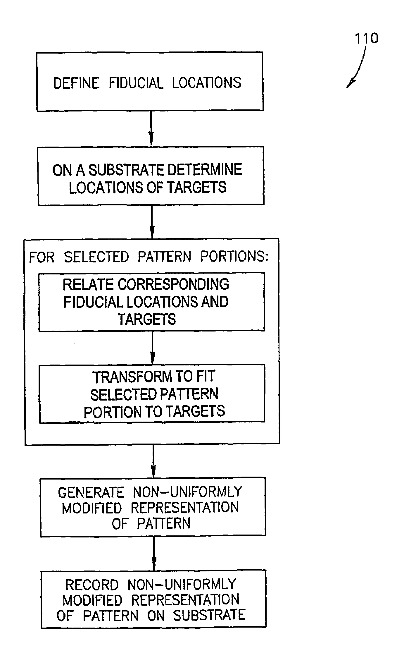
[0037]The invention will now be taught using various exemplary embodiments. Although the embodiments are described in detail, it will be appreciated that the invention is not limited to just these embodiments, but has a scope that is significantly broader. The appended claims should be consulted to determine the true scope of the invention.

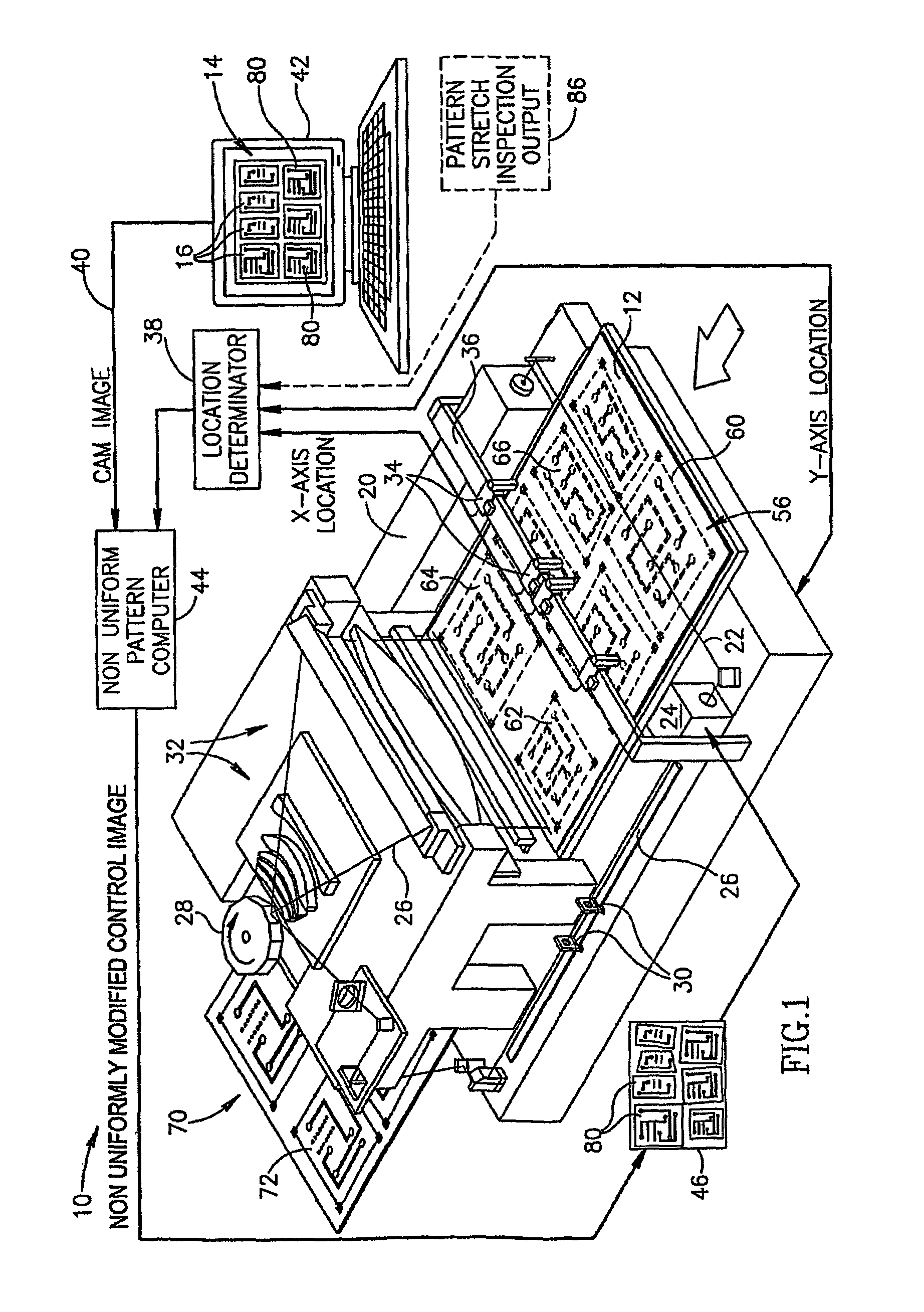
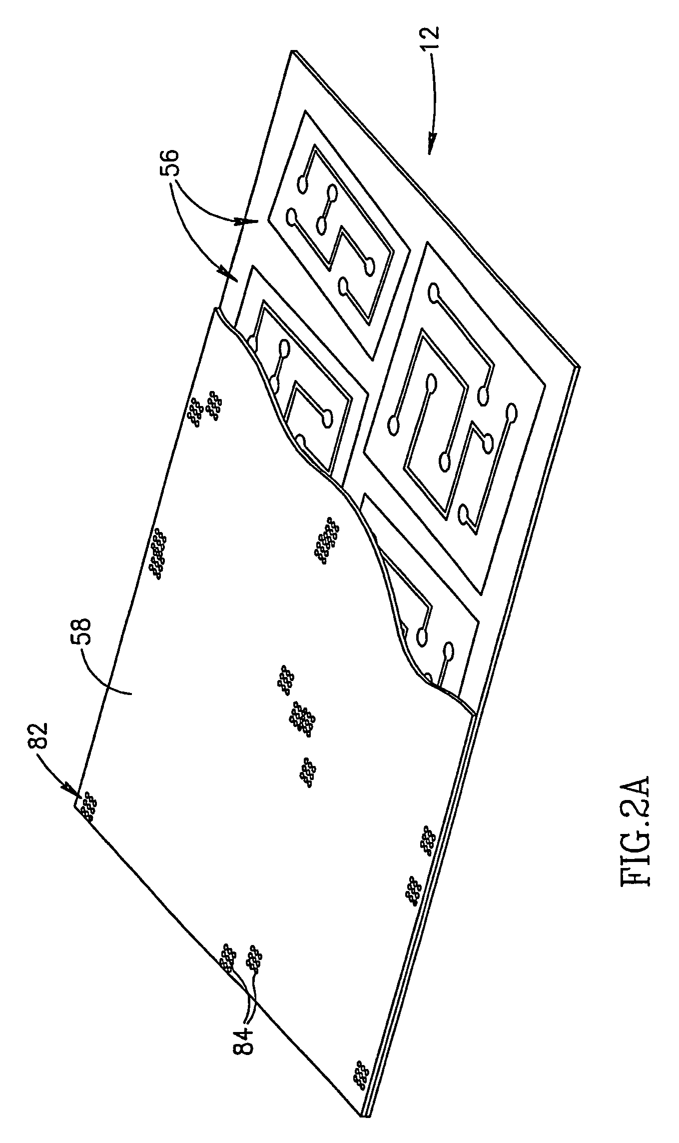
[0038]Reference is made to FIG. 1, which is a simplified pictorial illustration of a system 10 for exposing patterns on photosensitized surfaces of substrates 12, such as electrical circuit substrates, in accordance with an embodiment of the invention. As used in the following description, reference to electrical circuits includes any suitable form of electrical circuits, including printed circuit boards, ball grid array substrates, multi-chip modules, integrated circuits, and the like. Reference a direct imaging system includes, for example, a laser direct Imaging (LDI) system or in the alternative any suitable direct imaging system, for example ...


PUM

PropertyMeasurementUnit
electricalaaaaaaaaaa
photosensitiveaaaaaaaaaa
dimensionsaaaaaaaaaa

Abstract

A system and method for fabricating an electrical circuit in which a digital control image (46) is generated by non-uniformly modifying (44) a representation of an electrical circuit (40), such that an electrical circuit pattern (72) recorded on a substrate (12) using the digital control image (46) precisely fits an already formed electrical circuit portion (62).

Description

CROSS-REFERENCE TO RELATED APPLICATIONS.[0001]This application is a PCT application claiming priority from U.S. Provisional Application No. 60 / 376,874, filed May 2, 2002, which is incorporated by reference, herein, in its entirety.FIELD OF THE INVENTION.[0002]The following invention generally relates to printed circuit board manufacture, and more particularly to systems and methods that precisely record electrical circuit pattern portions on substrates.BACKGROUND OF THE INVENTION.[0003]A laser direct imaging (LDI) system suitable for recording electrical circuit pattern portions on photosensitive layers of electrical circuit substrates is commercially available from Orbotech Ltd. of Yavne Israel under the name DP-100™.[0004]Among the problems which arise during the manufacture of multi-layered printed circuit boards is that an electrical circuit pattern portion that is recorded on a substrate layer needs to have precise dimensions and needs to be precisely aligned on the substrate l...

Claims


Application Information

Patent Timeline
Patent Type & Authority Patents(United States)
IPC IPC(8): G01B11/00B41J2/435B41J2/47G03C5/00G03F9/00G06K9/00G03F7/20H05K1/02H05K3/00H05K3/46
CPCG03F7/2051H05K3/0082G03F9/00H05K1/0237H05K1/0269H05K3/0005H05K3/0008H05K2201/09918H05K2203/107G05B15/00
Inventor HANINA, GOLANGINO, HANANRUECKER, STEFFENBEN-TOV, IDO
Owner ORBOTECH LTD
Why Eureka
Try Eureka